|
|
|
PDF X40415 Data sheet ( Hoja de datos )
| Número de pieza | X40415 | |
| Descripción | (X40410 - X40415) Dual Voltage Monitor | |
| Fabricantes | Intersil Corporation | |
| Logotipo | ||
Hay una vista previa y un enlace de descarga de X40415 (archivo pdf) en la parte inferior de esta página. Total 24 Páginas | ||
|
No Preview Available !
®
Data Sheet
X40410, X40411, X40414, X40415
4kbit EEPROM
March 28, 2005
FN8116.0
Dual Voltage Monitor with Integrated CPU
Supervisor
FEATURES
• Dual voltage detection and reset assertion
—Standard reset threshold settings
See Selection table on page 2.
—Adjust low voltage reset threshold voltages
using special programming sequence
—Reset signal valid to VCC = 1V
—Monitor three voltages or detect power fail
• Independent Core Voltage Monitor (V2MON)
• Fault detection register
• Selectable power-on reset timeout (0.05s,
0.2s, 0.4s, 0.8s)
• Selectable watchdog timer interval (25ms,
200ms,1.4s, off)
• Low power CMOS
—25µA typical standby current, watchdog on
—6µA typical standby current, watchdog off
• 4Kbits of EEPROM
—16 byte page write mode
—5ms write cycle time (typical)
www.DataSheet4U.com
• Built-in inadvertent write protection
—Power-up/power-down protection circuitry
—Block lock protect none or 1/2 of EEPROM
• 400kHz 2-wire interface
• 2.7V to 5.5V power supply operation
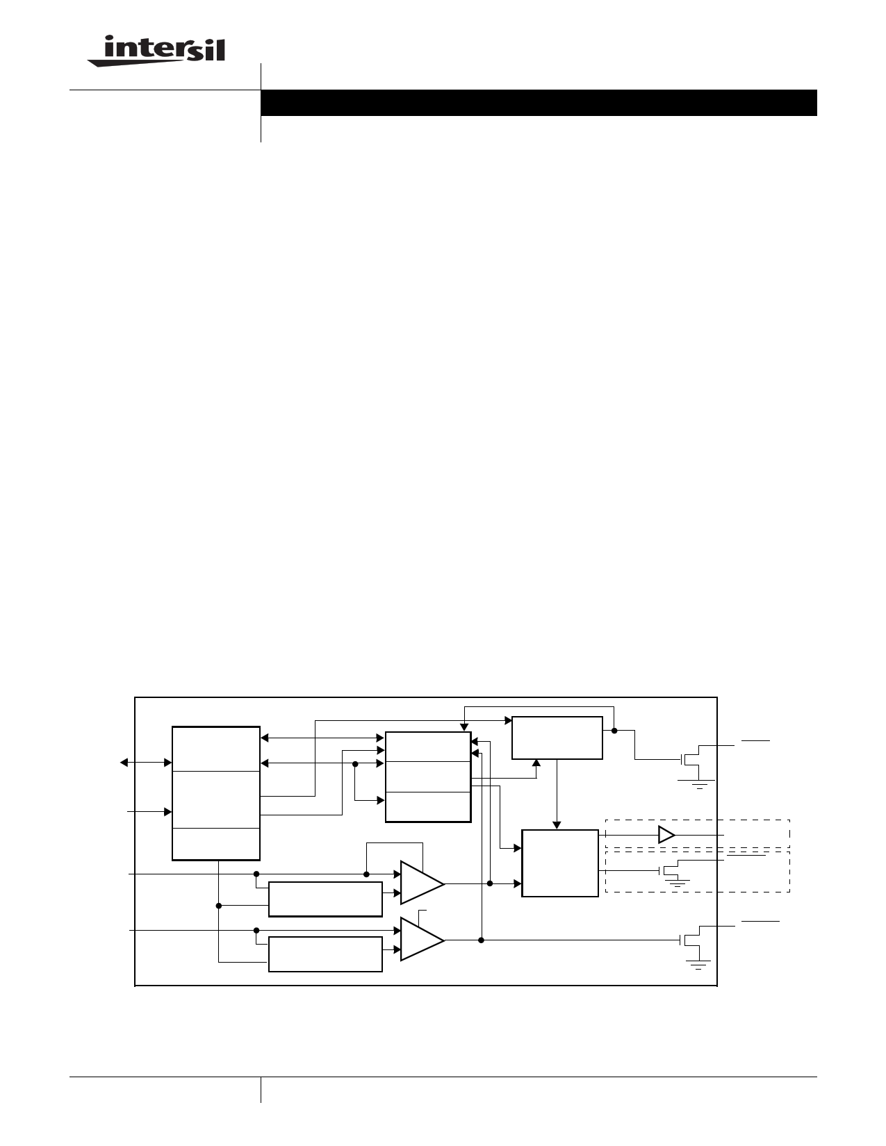
BLOCK DIAGRAM
• Available packages
—8-lead SOIC, TSSOP
• Monitor Voltages: 5V to 0.9V
• Memory Security
• Independent Core Voltage Monitor
APPLICATIONS
• Communication Equipment
—Routers, Hubs, Switches
—Disk Arrays, Network Storage
• Industrial Systems
—Process Control
—Intelligent Instrumentation
• Computer Systems
— Computers
—Network Servers
DESCRIPTION
The X40410/11/14/15 combines power-on reset con-
trol, watchdog timer, supply voltage supervision, and
secondary voltage supervision, and Block Lock™ pro-
tect serial EEPROM in one package. This combination
lowers system cost, reduces board space require-
ments, and increases reliability.
Applying voltage to VCC activates the power-on reset
circuit which holds RESET/RESET active for a period of
time. This allows the power supply and system oscilla-
SDA
SCL
VCC
(V1MON)
V2MON
Data
Register
Command
Decode Test
& Control
Logic
Threshold
Reset Logic
Fault Detection
Register
Status
Register
EEPROM
Array
Watchdog Timer
and
Reset Logic
User Programmable
VTRIP1
User Programmable
VTRIP2
+
-
VCC or
+ V2MON
Power-on,
Low Voltage
Reset
Generation
-
*X40410/11= V2MON*
X40414/15 = VCC
WDO
RESET
X40410/14
RESET
X40411/15
V2FAIL
1
CAUTION: These devices are sensitive to electrostatic discharge; follow proper IC Handling Procedures.
1-888-INTERSIL or 1-888-352-6832 | Intersil (and design) is a registered trademark of Intersil Americas Inc.
Copyright Intersil Americas Inc. 2005. All Rights Reserved
All other trademarks mentioned are the property of their respective owners.
1 page 
X40410, X40411, X40414, X40415
Resetting the VTRIPx Voltage
To reset a VTRIPx voltage, apply the programming volt-
age (Vp) to the WDO pin before a START condition is
set up on SDA. Next, issue on the SDA pin the Slave
Address A0h followed by the Byte Address 03h for
VTRIP1 and 0Bh for VTRIP2, followed by 00h for the
Data Byte in order to reset VTRIPx. The STOP bit fol-
lowing a valid write operation initiates the program-
ming sequence. Pin WDO must then be brought LOW
to complete the operation.
After being reset, the value of VTRIPx becomes a nomi-
nal value of 1.7V or lesser.
Note: This operation does not corrupt the memory
array.
CONTROL REGISTER
The Control Register provides the user a mechanism for
changing the Block Lock and Watchdog Timer settings.
The Block Lock and Watchdog Timer bits are nonvolatile
and do not change when power is removed.
The Control Register is accessed with a special pream-
ble in the slave byte (1011) and is located at address
1FFh. It can only be modified by performing a byte write
operation directly to the address of the register and only
one data byte is allowed for each register write operation.
Prior to writing to the Control Register, the WEL and
RWEL bits must be set using a two step process, with
the whole sequence requiring 3 steps. See "Writing to
the Control Registers" on page 7.
The user must issue a stop, after sending this byte to
the register, to initiate the nonvolatile cycle that stores
WD1, WD0, PUP1, PUP0, BP1, and BP0. The
X40410/11/14/15 will not acknowledge any data bytes
written after the first byte is entered.
The state of the Control Register can be read at any
time by performing a random read at address 01Fh,
using the special preamble. Only one byte is read by
each register read operation. The master should sup-
ply a stop condition to be consistent with the bus pro-
tocol, but a stop is not required to end this operation.
765 4
PUP1 WD1 WD0 BP
3 2 10
0 RWEL WEL PUP0
RWEL: Register Write Enable Latch (Volatile)
The RWEL bit must be set to “1” prior to a write to the
Control Register.
Figure 4. Sample VTRIP Reset Circuit
VTRIP1
Adj.
V2FAIL
RESET
VTRIP2
Adj.
4.7K
1
3 SOIC
2 X4041x
4
8
7
6
5
VP
Adjust
Run
µC
SCL
SDA
5 FN8116.0
March 28, 2005
5 Page 
X40410, X40411, X40414, X40415
Stops and Write Modes
Stop conditions that terminate write operations must
be sent by the master after sending at least 1 full data
byte plus the subsequent ACK signal. If a stop is
issued in the middle of a data byte, or before 1 full
data byte plus its associated ACK is sent, then the
device will reset itself without performing the write. The
contents of the array will not be effected.
Acknowledge Polling
The disabling of the inputs during high voltage cycles
can be used to take advantage of the typical 5ms write
cycle time. Once the stop condition is issued to indi-
cate the end of the master’s byte load operation, the
device initiates the internal high voltage cycle.
Acknowledge polling can be initiated immediately. To
do this, the master issues a start condition followed by
the Slave Address Byte for a write or read operation. If
the device is still busy with the high voltage cycle then
no ACK will be returned. If the device has completed
the write operation, an ACK will be returned and the
host can then proceed with the read or write operation.
See Figure 12.
Serial Read Operations
Read operations are initiated in the same manner as
write operations with the exception that the R/W bit of
the Slave Address Byte is set to one. There are three
basic read operations: Current Address Reads, Ran-
dom Reads, and Sequential Reads.
Current Address Read
Internally the device contains an address counter that
maintains the address of the last word read incre-
mented by one. Therefore, if the last read was to
address n, the next read operation would access data
from address n+1. On power-up, the address of the
address counter is undefined, requiring a read or write
operation for initialization.
Upon receipt of the Slave Address Byte with the R/W
bit set to one, the device issues an acknowledge and
then transmits the eight bits of the Data Byte. The
master terminates the read operation when it does not
respond with an acknowledge during the ninth clock
and then issues a stop condition. See Figure 13 for the
address, acknowledge, and data transfer sequence.
Figure 12. Acknowledge Polling Sequence
Byte Load Completed
by Issuing STOP.
Enter ACK Polling
Issue START
Issue Slave Address
Byte (Read or Write)
Issue STOP
ACK
Returned?
YES
NO
High Voltage Cycle
Complete. Continue
Command Sequence?
YES
Continue Normal
Read or Write
Command Sequence
Issue STOP
NO
PROCEED
It should be noted that the ninth clock cycle of the read
operation is not a “don’t care.” To terminate a read
operation, the master must either issue a stop condi-
tion during the ninth cycle or hold SDA HIGH during
the ninth clock cycle and then issue a stop condition.
Random Read
Random read operation allows the master to access any
memory location in the array. Prior to issuing the Slave
Address Byte with the R/W bit set to one, the master
must first perform a “dummy” write operation. The master
issues the start condition and the Slave Address Byte,
receives an acknowledge, then issues the Word Address
Bytes. After acknowledging receipts of the Word Address
Bytes, the master immediately issues another start con-
dition and the Slave Address Byte with the R/W bit set to
one. This is followed by an acknowledge from the device
and then by the eight bit word. The master terminates the
read operation by not responding with an acknowledge
and then issuing a stop condition. See Figure 14 for the
address, acknowledge, and data transfer sequence.
11 FN8116.0
March 28, 2005
11 Page | ||
| Páginas | Total 24 Páginas | |
| PDF Descargar | [ Datasheet X40415.PDF ] | |
Hoja de datos destacado
| Número de pieza | Descripción | Fabricantes |
| X40410 | (X40410 - X40415) Dual Voltage Monitor | Intersil Corporation |
| X40411 | (X40410 - X40415) Dual Voltage Monitor | Intersil Corporation |
| X40414 | (X40410 - X40415) Dual Voltage Monitor | Intersil Corporation |
| X40415 | (X40410 - X40415) Dual Voltage Monitor | Intersil Corporation |
| Número de pieza | Descripción | Fabricantes |
| SLA6805M | High Voltage 3 phase Motor Driver IC. |
Sanken |
| SDC1742 | 12- and 14-Bit Hybrid Synchro / Resolver-to-Digital Converters. |
Analog Devices |
|
DataSheet.es es una pagina web que funciona como un repositorio de manuales o hoja de datos de muchos de los productos más populares, |
| DataSheet.es | 2020 | Privacy Policy | Contacto | Buscar |