|
|
|
PDF XX1002 Data sheet ( Hoja de datos )
| Número de pieza | XX1002 | |
| Descripción | GaAs MMIC Active Doubler | |
| Fabricantes | Mimix Broadband | |
| Logotipo | ||
Hay una vista previa y un enlace de descarga de XX1002 (archivo pdf) en la parte inferior de esta página. Total 5 Páginas | ||
|
No Preview Available !
2.5-6.0/5.0-12.0 GHz GaAs MMIC
Active Doubler
December 2005 - Rev 08-Dec-05
Features
Compact, Low-Cost Design
Octave Bandwidth Operation
+16 dBm Output Power
-35 dBc Fundamental Leakage
+5.0V, 125mA Bias Supply
100% On-Wafer RF, DC and Output Power Testing
100% Visual Inspection to MIL-STD-883
Method 2010
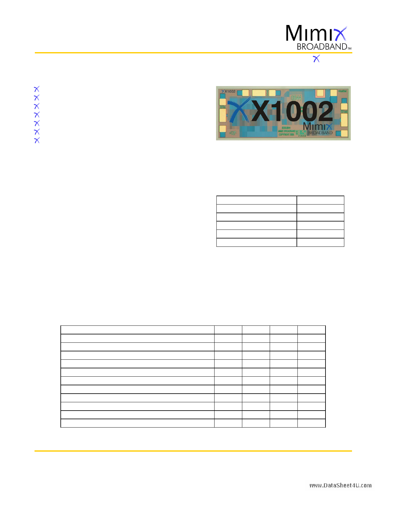
Chip Device Layout
X1002
General Description
Mimix Broadband's 2.5-6.0/5.0-12.0 GHz GaAs MMIC
Active Doubler delivers + 16 dBm of output power.
The circuit combines an active doubler with an
output buffer amplifier that delivers constant power
over a range of input powers. The circuit has excellent
rejection of the fundamental and harmonic products
and requires a single positive bias supply.This MMIC
uses Mimix Broadband's 2 um GaAs HBT device model
technology to ensure high reliability and uniformity.
The chip has surface passivation to protect and
provide a rugged part with backside via holes and
gold metallization to allow either a conductive epoxy
or eutectic solder die attach process.This device is
well suited for Millimeter-wave Point-to-Point Radio,
LMDS, SATCOM and VSAT applications.
Absolute Maximum Ratings
Supply Voltage (Vcc)
Supply Current (Id)
Input Power (RF Pin)
Storage Temperature (Tstg)
Operating Temperature (Ta)
Junction Temperature (Tj)
+6.0 VDC
200 mA
+10.0 dBm
-65 to +165 OC
-55 to MTTF Table1
MTTF Table1
(1) Junction temperature affects a device's MTTF. It is
recommended to keep junction temperature as low as
possible for maximum life.
Electrical Characteristics (Ambient Temperature T = 25 oC)
Parameter
Input Frequency Range (fin)
Output Frequency Range (fout)
Input Return Loss (S11)
Output Return Loss (S22)
Saturated Output Power (Psat)
RF Input Power (RF Pin)
Fundamental Leakage (fin)
Third Harmonic Leakage (3xfin)
Fourth Harmonic Leakage (4xfin)
Bias Voltage (Vcc)
Supply Current
Units Min. Typ. Max.
GHz 2.5 - 6.0
GHz 5.0
- 12.0
dB - -15 -
dB - TBD -
dBm - +16 -
dBm -3.0
- +3.0
dBc - -35 -
dBc - -30 -
dBc - -20 -
VDC - +5.0 +5.5
mA - 120 140
Mimix Broadband, Inc., 10795 Rockley Rd., Houston, Texas 77099
Tel: 281.988.4600 Fax: 281.988.4615 mimixbroadband.com
Page 1 of 5
Characteristic Data and Specifications are subject to change without notice. ©2005 Mimix Broadband, Inc.
Export of this item may require appropriate export licensing from the U.S. Government. In purchasing these parts, U.S. Domestic customers accept
their obligation to be compliant with U.S. Export Laws.
1 page 
2.5-6.0/5.0-12.0 GHz GaAs MMIC
Active Doubler
December 2005 - Rev 08-Dec-05
X1002
Handling and Assembly Information
CAUTION! - Mimix Broadband MMIC Products contain gallium arsenide (GaAs) which can be hazardous to the
human body and the environment. For safety, observe the following procedures:
Do not ingest.
Do not alter the form of this product into a gas, powder, or liquid through burning, crushing, or chemical
processing as these by-products are dangerous to the human body if inhaled, ingested, or swallowed.
Observe government laws and company regulations when discarding this product.This product must be
discarded in accordance with methods specified by applicable hazardous waste procedures.
Life Support Policy - Mimix Broadband's products are not authorized for use as critical components in life support
devices or systems without the express written approval of the President and General Counsel of Mimix
Broadband. As used herein: (1) Life support devices or systems are devices or systems which, (a) are intended for
surgical implant into the body, or (b) support or sustain life, and whose failure to perform when properly used in
accordance with instructions for use provided in the labeling, can be reasonably expected to result in a
significant injury to the user. (2) A critical component is any component of a life support device or system whose
failure to perform can be reasonably expected to cause the failure of the life support device or system, or to
affect its safety or effectiveness.
ESD - Gallium Arsenide (GaAs) devices are susceptible to electrostatic and mechanical damage. Die are supplied
in antistatic containers, which should be opened in cleanroom conditions at an appropriately grounded anti-
static workstation. Devices need careful handling using correctly designed collets, vacuum pickups or, with care,
sharp tweezers.
Die Attachment - GaAs Products from Mimix Broadband are 0.100 mm (0.004") thick and have vias through to the
backside to enable grounding to the circuit. Microstrip substrates should be brought as close to the die as
possible.The mounting surface should be clean and flat. If using conductive epoxy, recommended epoxies are
Ablestick 84-1LMI or 84-1LMIT cured in a nitrogen atmosphere per manufacturer's cure schedule. Apply epoxy
sparingly to avoid getting any on to the top surface of the die. An epoxy fillet should be visible around the total
die periphery. If eutectic mounting is preferred, then a fluxless gold-tin (AuSn) preform, approximately 0.0012
thick, placed between the die and the attachment surface should be used. A die bonder that utilizes a heated
collet and provides scrubbing action to ensure total wetting to prevent void formation in a nitrogen atmosphere
is recommended.The gold-tin eutectic (80% Au 20% Sn) has a melting point of approximately 280 C (Note: Gold
Germanium should be avoided).The work station temperature should be 310 C+- 10 C. Exposure to these
extreme temperatures should be kept to minimum.The collet should be heated, and the die pre-heated to avoid
excessive thermal shock. Avoidance of air bridges and force impact are critical during placement.
Wire Bonding - Windows in the surface passivation above the bond pads are provided to allow wire bonding to
the die's gold bond pads.The recommended wire bonding procedure uses 0.076 mm x 0.013 mm (0.003" x
0.0005") 99.99% pure gold ribbon with 0.5-2% elongation to minimize RF port bond inductance. Gold 0.025 mm
(0.001") diameter wedge or ball bonds are acceptable for DC Bias connections. Aluminum wire should be
avoided.Thermo-compression bonding is recommended though thermosonic bonding may be used providing
the ultrasonic content of the bond is minimized. Bond force, time and ultrasonics are all critical parameters.
Bonds should be made from the bond pads on the die to the package or substrate. All bonds should be as short
as possible.
Mimix Broadband, Inc., 10795 Rockley Rd., Houston, Texas 77099
Tel: 281.988.4600 Fax: 281.988.4615 mimixbroadband.com
Page 5 of 5
Characteristic Data and Specifications are subject to change without notice. ©2005 Mimix Broadband, Inc.
Export of this item may require appropriate export licensing from the U.S. Government. In purchasing these parts, U.S. Domestic customers accept
their obligation to be compliant with U.S. Export Laws.
5 Page | ||
| Páginas | Total 5 Páginas | |
| PDF Descargar | [ Datasheet XX1002.PDF ] | |
Hoja de datos destacado
| Número de pieza | Descripción | Fabricantes |
| XX1000 | GaAs MMIC Active Doubler | Mimix Broadband |
| XX1000-BD | GaAs MMIC Active Doubler | Mimix Broadband |
| XX1000-QT | Active Doubler | Mimix Broadband |
| XX1001-BD | GaAs MMIC Doubler and Power Amplifier | Mimix Broadband |
| Número de pieza | Descripción | Fabricantes |
| SLA6805M | High Voltage 3 phase Motor Driver IC. |
Sanken |
| SDC1742 | 12- and 14-Bit Hybrid Synchro / Resolver-to-Digital Converters. |
Analog Devices |
|
DataSheet.es es una pagina web que funciona como un repositorio de manuales o hoja de datos de muchos de los productos más populares, |
| DataSheet.es | 2020 | Privacy Policy | Contacto | Buscar |