|
|
|
PDF XU1009-BD Data sheet ( Hoja de datos )
| Número de pieza | XU1009-BD | |
| Descripción | GaAs MMIC Transmitter | |
| Fabricantes | Mimix Broadband | |
| Logotipo | ||
Hay una vista previa y un enlace de descarga de XU1009-BD (archivo pdf) en la parte inferior de esta página. Total 9 Páginas | ||
|
No Preview Available !
18.0-36.0 GHz GaAs MMIC
Transmitter
March 2007 - Rev 01-Mar-07
Features
Sub-harmonic Transmitter
Integrated Mixer, LO Doubler/Buffer & Output Amplifier
+25.0 dBm Output Third Order Intercept (OIP3)
35.0 dB Gain Control
2.0 dBm LO Drive Level
9.0 dB Conversion Gain
100% On-Wafer RF and DC Testing
100% Visual Inspection to MIL-STD-883 Method 2010
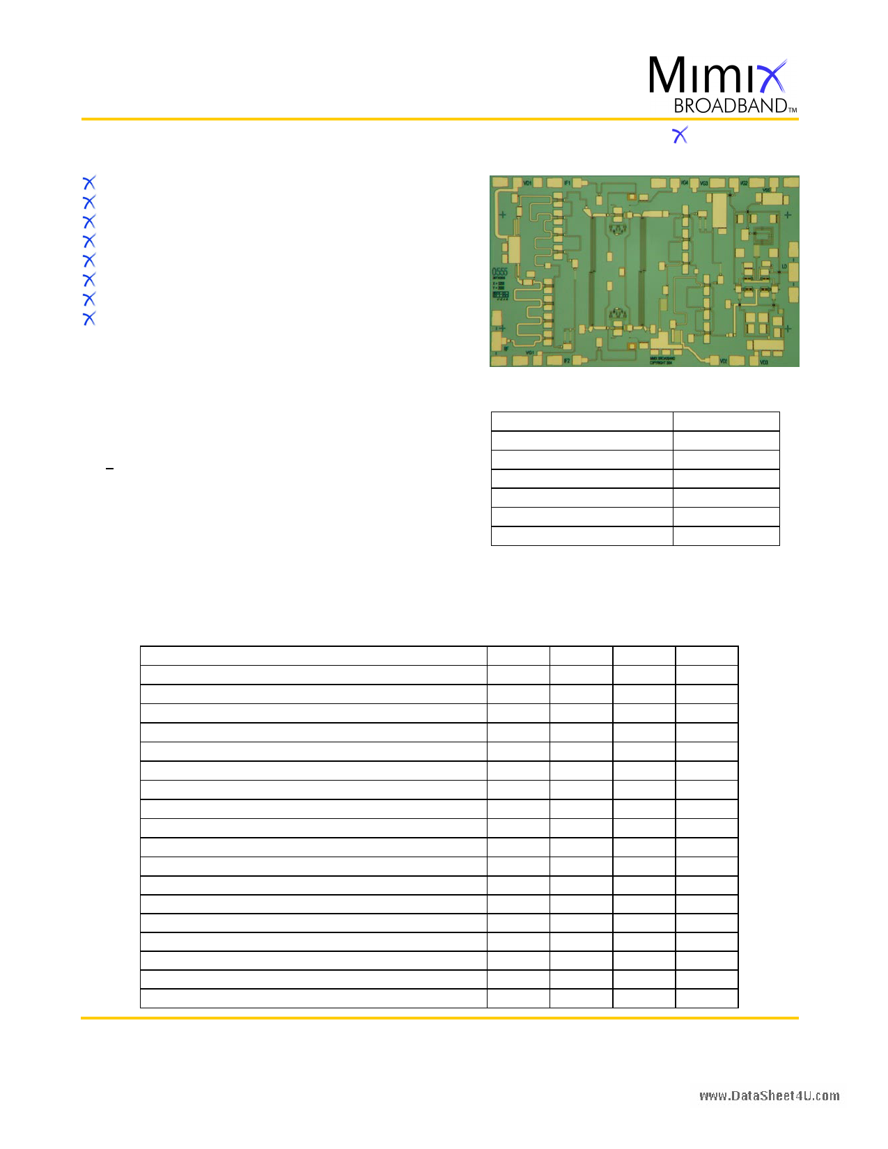
U1009-BD
Chip Device Layout
General Description
Mimix Broadband’s 18.0-36.0 GHz GaAs MMIC transmitter has a +25.0
dBm output third order intercept across the band.This device is a
balanced resistive pHEMT mixer followed by a distributed amplifier
and includes an integrated LO doubler and LO buffer amplifier.The use
of integrated LO doubler and LO buffer amplifier makes the provision
of the LO easier than for fundamental mixers at these frequencies. IF
and IF mixer inputs are provided through an external 180 degree
hybrid.This MMIC uses Mimix Broadband’s 0.15 µm GaAs PHEMT
device model technology, and is based upon electron beam
lithography to ensure high repeatability and uniformity.The chip has
surface passivation to protect and provide a rugged part with backside
via holes and gold metallization to allow either a conductive epoxy or
eutectic solder die attach process.This device is well suited for
Millimeter-wave Point-to-Point Radio, LMDS, SATCOM and VSAT
applications.
XU1009-BD
Absolute Maximum Ratings
Supply Voltage (Vd)
Supply Current (Id1,2,3)
Gate Bias Voltage (Vg)
Input Power (IF Pin)
Storage Temperature (Tstg)
Operating Temperature (Ta)
Channel Temperature (Tch)
+6.0 VDC
320,190,110 mA
+0.3 VDC
0.0 dBm
-65 to +165 OC
-55 to MTTF Table3
MTTF Table3
(1) Measured using constant current.
(2) Measured using LO Input drive level of +2.0 dBm.
(3) Channel temperature affects a device's MTTF. It is
recommended to keep channel temperature as low as
possible for maximum life.
Electrical Characteristics (Ambient Temperature T = 25o C)
Parameter
Units Min. Typ. Max.
Frequency Range (RF) Upper Side Band
GHz 18.0 - 36.0
Frequency Range (RF) Lower Side Band
GHz 18.0 - 36.0
Frequency Range (LO)
GHz 8.0
- 19.5
Frequency Range (IF)
GHz DC - 3.0
Output Return Loss RF (S22)
Small Signal Conversion Gain IF/RF (S21) 2
dB - 14.0 -
dB - 9.0 -
LO Input Drive (PLO)
dBm - +2.0 -
Isolation LO/RF @ LOx1
dB - 15.0 -
Isolation LO/RF @ LOx2
Output Third Order Intercept (OIP3)1,2
dB - 5.0 -
dBm - +25.0 -
Drain Bias Voltage (Vd1,2,3)
VDC - +5.0 +5.5
Source Bias Voltage (Vss)
VDC - -5.0 -
Gate Bias Voltage (Vg1,2)
VDC -1.2 -0.2 +0.1
Gate Bias Voltage (Vg3,4) Doubler, Mixer
Supply Current (Id1) (Vd1=5.0V, Vg=-0.2V Typical)
Supply Current (Id2) (Vd2=5.0V, Vg=-0.1V Typical)
Supply Current (Id3) (Vd3=5.0V, Vg=-0.5V Typical)
Supply Current (Iss) (Vss=-5.0V)
VDC -1.2 -0.5 +0.1
mA - 230 280
mA - 140 170
mA -
75 90
mA -
50 60
Mimix Broadband, Inc., 10795 Rockley Rd., Houston, Texas 77099
Tel: 281.988.4600 Fax: 281.988.4615 mimixbroadband.com
Page 1 of 9
Characteristic Data and Specifications are subject to change without notice. ©2007 Mimix Broadband, Inc.
Export of this item may require appropriate export licensing from the U.S. Government. In purchasing these parts, U.S. Domestic customers accept
their obligation to be compliant with U.S. Export Laws.
1 page 
18.0-36.0 GHz GaAs MMIC
Transmitter
March 2007 - Rev 01-Mar-07
Mechanical Drawing
0.305
(0.012)
2.000
(0.079)
2
0.904
(0.036)
3
1.904 2.104 2.504
2.904
(0.075) (0.083) (0.099) (0.114)
45 6 7
U1009-BD
8
0.996
(0.039)
0.295
(0.012)
0.0
1
0.0
12 11
XU1009-BD
10 9
0.504
0.904
(0.020) (0.036)
2.305 2.704
(0.091) (0.106)
(Note: Engineering designator is 26TX0555)
3.200
(0.126)
Units: millimeters (inches) Bond pad dimensions are shown to center of bond pad.
Thickness: 0.110 +/- 0.010 (0.0043 +/- 0.0004), Backside is ground, Bond Pad/Backside Metallization: Gold
All DC/IF Bond Pads are 0.100 x 0.100 (0.004 x 0.004). All RF Bond Pads are 0.100 x 0.200 (0.004 x 0.008).
Bond pad centers are approximately 0.109 (0.004) from the edge of the chip.
Dicing tolerance: +/- 0.005 (+/- 0.0002). Approximate weight: 3.968 mg.
Bond Pad #1 (RF Out) Bond Pad #3 (IF1) Bond Pad #5 (Vg3) Bond Pad #7 (Vss) Bond Pad #9 (Vd3) Bond Pad #11 (IF2)
Bond Pad #2 (Vd1) Bond Pad #4 (Vg4) Bond Pad #6 (Vg2) Bond Pad #8 (LO) Bond Pad #10 (Vd2) Bond Pad #12 (Vg1)
Bias Arrangement
Vd1 Vg4
IF1
23
45
Vg3
Vg2
67
Vss
Bypass Capacitors - See App Note [2]
8 LO
RF 1
12 11
IF2
Vg1
Vd2
XU1009-BD
10 9
Vd3
Mimix Broadband, Inc., 10795 Rockley Rd., Houston, Texas 77099
Tel: 281.988.4600 Fax: 281.988.4615 mimixbroadband.com
Page 5 of 9
Characteristic Data and Specifications are subject to change without notice. ©2007 Mimix Broadband, Inc.
Export of this item may require appropriate export licensing from the U.S. Government. In purchasing these parts, U.S. Domestic customers accept
their obligation to be compliant with U.S. Export Laws.
5 Page | ||
| Páginas | Total 9 Páginas | |
| PDF Descargar | [ Datasheet XU1009-BD.PDF ] | |
Hoja de datos destacado
| Número de pieza | Descripción | Fabricantes |
| XU1009-BD | GaAs MMIC Transmitter | Mimix Broadband |
| Número de pieza | Descripción | Fabricantes |
| SLA6805M | High Voltage 3 phase Motor Driver IC. |
Sanken |
| SDC1742 | 12- and 14-Bit Hybrid Synchro / Resolver-to-Digital Converters. |
Analog Devices |
|
DataSheet.es es una pagina web que funciona como un repositorio de manuales o hoja de datos de muchos de los productos más populares, |
| DataSheet.es | 2020 | Privacy Policy | Contacto | Buscar |