|
|
|
PDF ISL22426 Data sheet ( Hoja de datos )
| Número de pieza | ISL22426 | |
| Descripción | Dual Digitally Controlled Potentiometer | |
| Fabricantes | Intersil Corporation | |
| Logotipo | ||
Hay una vista previa y un enlace de descarga de ISL22426 (archivo pdf) en la parte inferior de esta página. Total 13 Páginas | ||
|
No Preview Available !
ISL22426
® Dual Digitally Controlled Potentiometer (XDCP™)
Data Sheet
July 17, 2006
FN6180.0
Low Noise, Low Power, SPI® Bus, 128 Taps
The ISL22426 integrates two digitally controlled
potentiometers (DCP) and non-volatile memory on a
monolithic CMOS integrated circuit.
The digitally controlled potentiometers are implemented with
a combination of resistor elements and CMOS switches. The
position of the wipers are controlled by the user through the
SPI serial interface. Each potentiometer has an associated
volatile Wiper Register (WR) and a non-volatile Initial Value
Register (IVR) that can be directly written to and read by the
user. The contents of the WR controls the position of the
wiper. At power-up the device recalls the contents of the
DCP’s IVR to the corresponding WR.
The DCPs can be used as three-terminal potentiometers or
as two-terminal variable resistors in a wide variety of
applications including control, parameter adjustments, and
signal processing.
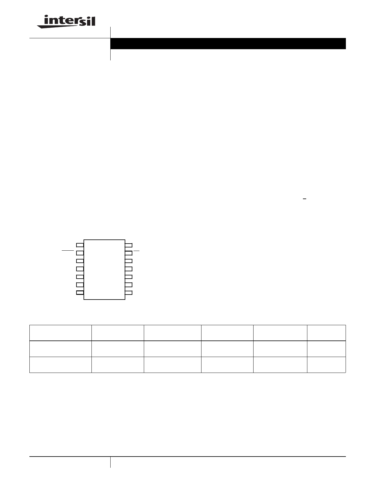
Pinout
www.DataSheet4U.com
VCC
SHDN
RH0
RL0
RW0
NC
SCK
ISL22426
(14 LEAD TSSOP)
TOP VIEW
1 14
2 13
3 12
4 11
5 10
69
78
SDI
CS
RH1
RL1
RW1
GND
SDO
Features
• Two potentiometers in one package
• 128 resistor taps
• SPI serial interface
• Non-volatile storage of wiper position
• Wiper resistance: 70Ω typical @ 3.3V
• Shutdown mode
• Shutdown current 5µA max
• Power supply: 2.7V to 5.5V
• 50kΩ or 10kΩ total resistance
• High reliability
- Endurance: 1,000,000 data changes per bit per register
- Register data retention: 50 years @ T <55°C
• 14 Lead TSSOP
• Pb-free plus anneal product (RoHS compliant)
Ordering Information
PART NUMBER
PART MARKING
RESISTANCE OPTION
(kΩ)
TEMP. RANGE
(°C)
PACKAGE
PKG. DWG. #
ISL22426UFV14Z
(Notes 1, 2)
22426 UFVZ
50
-40 to +125
14 Ld TSSOP
M14.173
(Pb-free)
ISL22426WFV14Z
(Notes 1, 2)
22426 WFVZ
10
-40 to +125
14 Ld TSSOP
M14.173
(Pb-free)
NOTES:
1. Intersil Pb-free plus anneal products employ special Pb-free material sets; molding compounds/die attach materials and 100% matte tin plate
termination finish, which are RoHS compliant and compatible with both SnPb and Pb-free soldering operations. Intersil Pb-free products are
MSL classified at Pb-free peak reflow temperatures that meet or exceed the Pb-free requirements of IPC/JEDEC J STD-020.
2. Add “-TK” suffix for 1,000 Tape and Reel option
1 CAUTION: These devices are sensitive to electrostatic discharge; follow proper IC Handling Procedures.
1-888-INTERSIL or 1-888-468-3774 | Intersil (and design) and XDCP are registered trademarks of Intersil Americas Inc.
Copyright Intersil Americas Inc. 2005. All Rights Reserved
All other trademarks mentioned are the property of their respective owners.
1 page 
ISL22426
Operating Specifications Over the recommended operating conditions unless otherwise specified. (Continued)
SYMBOL
PARAMETER
TEST CONDITIONS
TYP
MIN (NOTE 5) MAX
UNIT
EEPROM SPECIFICATION
EEPROM Endurance
1,000,000
Cycles
EEPROM Retention
Temperature T ≤ 55 °C
50
Years
tWC Non-volatile Write cycle time
(Note 19)
12 20 ms
SERIAL INTERFACE SPECIFICATIONS
VIL SHDN, SCK, SDI, and CS input buffer
LOW voltage
-0.3
0.3*VCC
V
VIH SHDN, SCK, SDI, and CS input buffer
HIGH voltage
0.7*VCC
VCC+0.3
V
Hysteresis SHDN, SCK, SDI, and CS input buffer
hysteresis
0.05*
VCC
V
VOL SDO output buffer LOW voltage
IOL = 4mA
0 0.4 V
Rpu SDO pull-up resistor off-chip
(Note 20)
Maximum is determined by tRO and tFO with
maximum bus load Cb = 30pF, fSCK = 5MHz
2 kΩ
Cpin SHDN, SCK, SDI, SDO and CS pin
(Note 21) capacitance
10 pF
fSCK
SPI frequency
5 MHz
tCYC
SPI clock cycle time
200 ns
tWH SPI clock high time
100 ns
tWL SPI clock low time
100 ns
tLEAD Lead time
250 ns
tLAG
Lag time
250 ns
tSU SDI, SCK and CS input setup time
50 ns
tH SDI, SCK and CS input hold time
50 ns
tRI SDI, SCK and CS input rise time
10 ns
tFI SDI, SCK and CS input fall time
10 20 ns
tDIS SDO output Disable time
0 100 ns
tV SDO output valid time
350 ns
tHO SDO output hold time
0 ns
tRO SDO output rise time
Rpu = 2k, Cb = 30pF
60 ns
tFO SDO output fall time
Rpu = 2k, Cb = 30pF
60 ns
tCS
NOTES:
CS deselect time
2 µs
5. Typical values are for TA = +25°C and 3.3V supply voltage.
6. LSB: [V(RW)127 – V(RW)0]/127. V(RW)127 and V(RW)0 are V(RW) for the DCP register set to 7F hex and 00 hex respectively. LSB is the
incremental voltage when changing from one tap to an adjacent tap.
7. ZS error = V(RW)0/LSB.
8. FS error = [V(RW)127 – VCC]/LSB.
9. DNL = [V(RW)i – V(RW)i-1]/LSB-1, for i = 1 to 127. i is the DCP register setting.
10. INL = [V(RW)i – i • LSB – V(RW)]/LSB for i = 1 to 127
11. VMATCH = [V(RWx)i – V(RWy)i]/LSB, for i = 1 to 127, x = 0 or 1 and y = 0 or 1.
12.
TCV
=
-------M-----a----x----(--V----(---R-----W------)--i--)---–-----M-----i--n----(--V-----(--R-----W------)--i--)------ × ----1---0----6----- for i = 16 to 112 decimal, T = -40°C to +125°C. Max( ) is the maximum value of the wiper
[Max(V(RW)i) + Min(V(RW)i)] ⁄ 2 165°C voltage and Min ( ) is the minimum value of the wiper voltage over the temperature range.
5 FN6180.0
July 17, 2006
5 Page 
ISL22426
Protocol Conventions
The first byte sent to the ISL22426 from the SPI host is the
Identification Byte. A valid Identification Byte contains 0101
as the four MSBs, with the following four bits set to 0.
TABLE 3. IDENTIFICATION BYTE FORMAT
01010000
(MSB)
(LSB)
The next byte sent to the ISL22426 contains the instruction
and register pointer information. The four MSBs are the
instruction and four LSBs are register address (see Table 4).
TABLE 4. IDENTIFICATION BYTE FORMAT
76543210
I3 I2 I1 I0 R3 R2 R1 R0
There are only two valid instruction sets:
1011(binary) - is a Read operation
1100(binary) - is a Write operation
Write Operation
A Write operation to the ISL22426 is a three-byte operation.
It requires first, the CS transition from HIGH to LOW, then a
valid Identification Byte, then a valid instruction byte
following by Data Byte is sent to SDI pin. The host
terminates the write operation by pulling the CS pin from
LOW to HIGH. For a write to addresses 0000b or 0001b, the
MSB at address 8 (ACR[7]) determines if the Data Byte is to
be written to volatile or both volatile and non-volatile
registers. Refer to “Memory Description” and Figure 16.
Device can receive more than one byte of data by auto
incrementing the address after each received byte. Note
after reaching the address 0110b, the internal pointer “rolls
over” to address 0000b.
The internal non-volatile write cycle starts after rising edge of
CS and takes up to 20ms. Thus, non-volatile registers must
be written individually.
Read Operation
A read operation to the ISL22426 is a three-byte operation. It
requires first, the CS transition from HIGH to LOW, then a
valid Identification Byte, then a valid instruction byte
following by “dummy” Data Byte is sent to SDI pin. The SPI
host reads the data from SDO pin on falling edge of SCK.
The host terminates the read operation by pulling the CS pin
from LOW to HIGH (see Figure 17).
The ISL22426 will provide the Data Bytes to the SDO pin as
long as SCK is provided by the host from the registers
indicated by an internal pointer. This pointer initial value is
determined by the register address in the Read operation
instruction, and increments by one during transmission of
each Data Byte. After reaching the memory location 0110b,
the pointer “rolls over” to 0000b, and the device continues to
output the data for each received SCK clock.
In order to read back the non-volatile IVR, it is recommended
that the application reads the ACR first to verify the WIP bit
is 0. If the WIP bit (ACR[5]) is not 0, the host should repeat
its reading sequence again.
CS
SCK
SDI
0 1 0 1 0 0 0 0 0 I3 I2 I1 I0 R3 R2 R1 R0
0 D6 D5 D4 D3 D2 D1 D0
FIGURE 16. THREE BYTE WRITE SEQUENCE
CS
SCK
SDI
SDO
0 1 0 1 0 0 0 0 0 I3 I2 I1 I0 R3 R2 R1 R0
DON’T CARE
0 D6 D5 D4 D3 D2 D1 D0
FIGURE 17. THREE BYTE READ SEQUENCE
11 FN6180.0
July 17, 2006
11 Page | ||
| Páginas | Total 13 Páginas | |
| PDF Descargar | [ Datasheet ISL22426.PDF ] | |
Hoja de datos destacado
| Número de pieza | Descripción | Fabricantes |
| ISL22424 | Dual Digitally Controlled Potentiometer | Intersil |
| ISL22426 | Dual Digitally Controlled Potentiometer | Intersil Corporation |
| ISL22429 | Dual Digitally Controlled Potentiometer | Intersil Corporation |
| Número de pieza | Descripción | Fabricantes |
| SLA6805M | High Voltage 3 phase Motor Driver IC. |
Sanken |
| SDC1742 | 12- and 14-Bit Hybrid Synchro / Resolver-to-Digital Converters. |
Analog Devices |
|
DataSheet.es es una pagina web que funciona como un repositorio de manuales o hoja de datos de muchos de los productos más populares, |
| DataSheet.es | 2020 | Privacy Policy | Contacto | Buscar |