|
|
|
PDF ADF4113HV Data sheet ( Hoja de datos )
| Número de pieza | ADF4113HV | |
| Descripción | High Voltage Charge Pump / PLL Synthesizer | |
| Fabricantes | Analog Devices | |
| Logotipo | ||
Hay una vista previa y un enlace de descarga de ADF4113HV (archivo pdf) en la parte inferior de esta página. Total 21 Páginas | ||
|
No Preview Available !
Data Sheet
High Voltage
Charge Pump, PLL Synthesizer
ADF4113HV
FEATURES
High voltage charge pump (15 V)
2.7 V to 5.5 V power supply
200 MHz to 4.0 GHz frequency range
Pin compatible with ADF4110, ADF4111, ADF4112, ADF4113
ADF4106, and ADF4002 synthesizers
Two selectable charge pump currents
Digital lock detect
Power-down mode
Loop filter design possible with ADIsimPLL™
APPLICATIONS
Applications using high voltage VCOs
IF/RF local oscillator (LO) generation in base stations
Point-to-point radio LO generation
Clock for analog-to-digital and digital-to-analog converters
Wireless LANs, PMR
Communications test equipment
GENERAL DESCRIPTION
The ADF4113HV is an integer-N frequency synthesizer with a
high voltage charge pump (15 V). The synthesizer is designed
for use with voltage controlled oscillators (VCOs) that have
high tuning voltages (up to 15 V). Active loop filters are often
used to achieve high tuning voltages, but the ADF4113HV
charge pump can drive a high voltage VCO directly with a
passive-loop filter. The ADF4113HV can be used to implement
local oscillators in the upconversion and downconversion
sections of wireless receivers and transmitters. It consists of a
low noise digital phase frequency detector (PFD), a precision
high voltage charge pump, a programmable reference divider,
programmable A and B counters, and a dual-modulus prescaler
(P/P + 1).
A simple 3-wire interface controls all of the on-chip registers.
The devices operate with a power supply ranging from 2.7 V to
5.5 V and can be powered down when not in use.
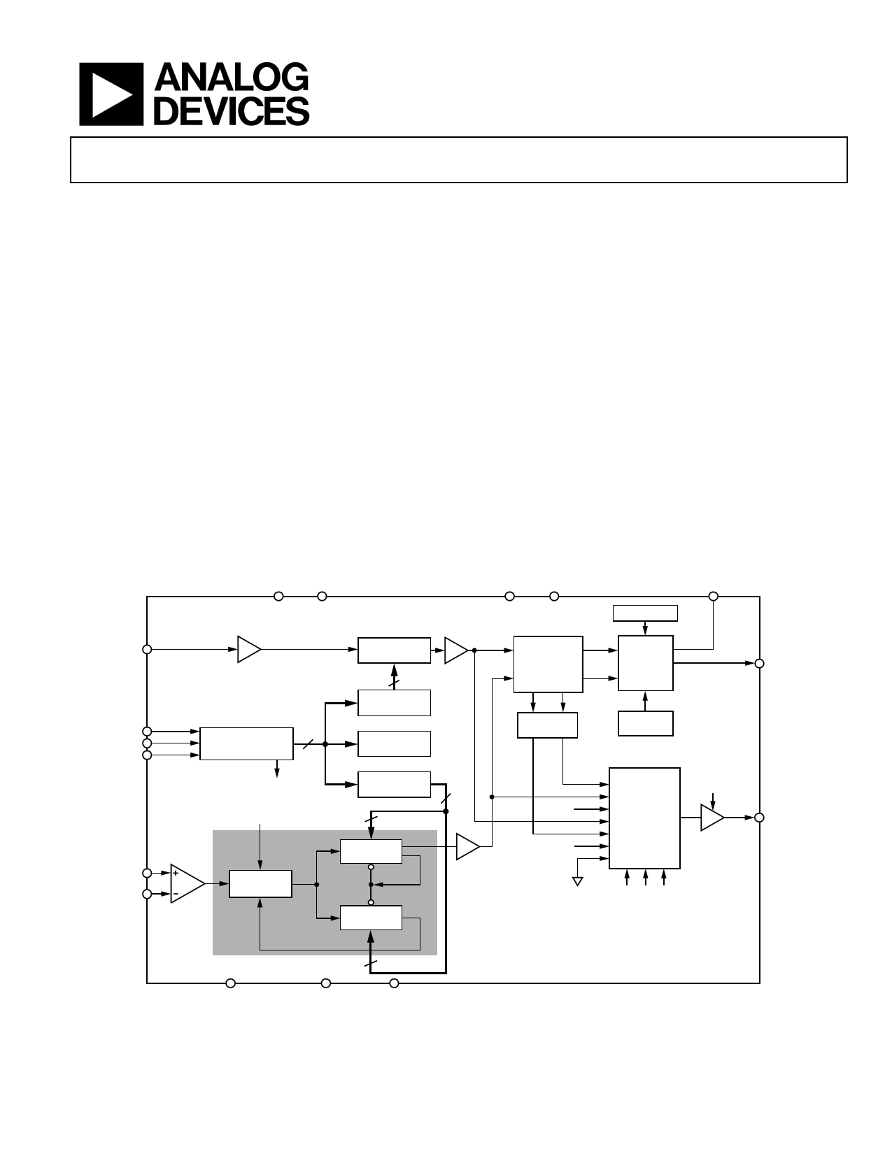
FUNCTIONAL BLOCK DIAGRAM
AVDD
DVDD
VP CPGND
REFERENCE
RSET
REFIN
CLK
DATA
LE
RFINA
RFINB
14-BIT
R COUNTER
14
R COUNTER
LATCH
24-BIT
INPUT REGISTER
22
FUNCTION
LATCH
SDOUT
FROM
FUNCTION
LATCH
N = BP + A
PRESCALER
P/P + 1
A, B COUNTER
LATCH
13
13-BIT
B COUNTER
LOAD
LOAD
6-BIT
A COUNTER
19
6
PHASE
FREQUENCY
DETECTOR
LOCK
DETECT
CHARGE
PUMP
CURRENT
SETTING
CP
AVDD
SDOUT
MUX
HIGH Z
MUXOUT
M3 M2 M1
ADF4113HV
CE
AGND
DGND
Figure 1.
Rev. B
Document Feedback
Information furnished by Analog Devices is believed to be accurate and reliable. However, no
responsibilityisassumedbyAnalogDevices for itsuse,nor foranyinfringementsofpatentsor other
rights of third parties that may result from its use. Specifications subject to change without notice. No
license is granted by implication or otherwise under any patent or patent rights of Analog Devices.
Trademarksandregisteredtrademarksarethepropertyoftheirrespectiveowners.
One Technology Way, P.O. Box 9106, Norwood, MA 02062-9106, U.S.A.
Tel: 781.329.4700 ©2007–2012 Analog Devices, Inc. All rights reserved.
Technical Support
www.analog.com
1 page 
ADF4113HV
Data Sheet
TIMING CHARACTERISTICS
Guaranteed by design but not production tested. AVDD = DVDD = 3 V ± 10%, 5 V ± 10%; 13.5 V ≤ VP ≤ 16.5 V;
AGND = DGND = CPGND = 0 V; RSET = 4.7 kΩ; TA = TMIN to TMAX, unless otherwise noted.
Table 2.
Parameter
t1
t2
t3
t4
t5
t6
t7
Limit at TMIN to TMAX (B Version)
20
10
10
25
25
10
20
Unit
ns min
ns min
ns min
ns min
ns min
ns min
ns min
Test Conditions/Comments
LE setup time
DATA to CLK setup time
DATA to CLK hold time
CLK high duration
CLK low duration
CLK to LE setup time
LE pulse width
Timing Diagram
CLK
t4 t5
DATA
DB23 (MSB)
LE
t1
LE
t2 t3
DB22
DB2
DB1
(CONTROL BIT C2)
Figure 2. Timing Diagram
DB0 (LSB)
(CONTROL BIT C1)
t7
t6
Rev. B | Page 4 of 20
5 Page 
ADF4113HV
PHASE FREQUENCY DETECTOR (PFD) AND
CHARGE PUMP
The PFD takes inputs from the R counter and N counter and
produces an output proportional to the phase and frequency
difference between them. Figure 17 is a simplified schematic.
The PFD includes a programmable delay element that controls
the width of the antibacklash pulse. This pulse ensures that
there is no dead zone in the PFD transfer function and mini-
mizes phase noise and reference spurs. Two bits in the reference
counter latch, ABP2 and ABP1, control the width of the pulse.
See Figure 20. The only recommended setting for the antiback-
lash pulse width is 7.2 ns.
HIGH
UP
D1 Q1
U1
VP CHARGE
PUMP
R DIVIDER
CLR1
PROGRAMMABLE
DELAY
U3
ABP1
ABP2
HIGH
N DIVIDER
CLR2
DOWN
D2 Q2
U2
CP
CPGND
R DIVIDER
N DIVIDER
CP OUTPUT
Figure 17. PFD Simplified Schematic and Timing (in Lock)
MUXOUT AND LOCK DETECT
The output multiplexer on the ADF4113HV allows the user to
access various internal points on the chip. The state of MUXOUT
is controlled by M3, M2, and M1 in the function latch. Figure 22
shows the full truth table (function latch map). Figure 18 shows
the MUXOUT section in block diagram form.
Data Sheet
DVDD
ANALOG LOCK DETECT
DIGITAL LOCK DETECT
R COUNTER OUTPUT
N COUNTER OUTPUT
SDOUT
MUX
CONTROL
MUXOUT
Figure 18. MUXOUT Circuit
DGND
Lock Detect
MUXOUT can be programmed for two types of lock detect:
digital lock detect and analog lock detect.
Digital lock detect is active high. When LDP in the AB counter
latch is set to 0, digital lock detect is set high when the phase
error on five consecutive phase detector (PD) cycles is less than
10 ns. With LDP set to 1, five consecutive cycles of less than
3 ns are required to set the lock detect. It stays high until a phase
error greater than 25 ns is detected on any subsequent PD cycle.
Operate the N-channel, open-drain, analog lock detect with a
10 kΩ nominal external pull-up resistor. When lock has been
detected, this output is high with narrow low-going pulses.
INPUT SHIFT REGISTER
The ADF4113HV digital section includes a 24-bit input shift
register, a 14-bit R counter, and a 19-bit N counter comprising
a 6-bit A counter and a 13-bit B counter. Data is clocked into
the 24-bit shift register on each rising edge of CLK, MSB first.
Data is transferred from the shift register to one of three latches
on the rising edge of LE. The destination latch is determined by
the state of the two control bits (C2, C1) in the shift register.
These are the two LSBs, DB1 and DB0, as shown in Figure 2.
The truth table for these bits is shown in Table 6. Figure 19
shows a summary of how the latches are programmed.
Table 6. C2, C1 Truth Table
Control Bits
C2 C1 Data Latch
0 0 R counter
0 1 N counter (A and B)
1 0 Function latch (including prescaler)
Rev. B | Page 10 of 20
11 Page | ||
| Páginas | Total 21 Páginas | |
| PDF Descargar | [ Datasheet ADF4113HV.PDF ] | |
Hoja de datos destacado
| Número de pieza | Descripción | Fabricantes |
| ADF4113HV | High Voltage Charge Pump / PLL Synthesizer | Analog Devices |
| Número de pieza | Descripción | Fabricantes |
| SLA6805M | High Voltage 3 phase Motor Driver IC. |
Sanken |
| SDC1742 | 12- and 14-Bit Hybrid Synchro / Resolver-to-Digital Converters. |
Analog Devices |
|
DataSheet.es es una pagina web que funciona como un repositorio de manuales o hoja de datos de muchos de los productos más populares, |
| DataSheet.es | 2020 | Privacy Policy | Contacto | Buscar |