|
|
|
PDF AD8318 Data sheet ( Hoja de datos )
| Número de pieza | AD8318 | |
| Descripción | Logarithmic Detector/Controller | |
| Fabricantes | Analog Devices | |
| Logotipo | ||
Hay una vista previa y un enlace de descarga de AD8318 (archivo pdf) en la parte inferior de esta página. Total 25 Páginas | ||
|
No Preview Available !
1 MHz to 8 GHz, 70 dB
Logarithmic Detector/Controller
AD8318
FEATURES
Wide bandwidth: 1 MHz to 8 GHz
High accuracy: ±1.0 dB over 55 dB range (f < 5.8 GHz)
Stability over temperature: ±0.5 dB
Low noise measurement/controller output (VOUT)
Pulse response time: 10 ns/12 ns (fall/rise)
Integrated temperature sensor
Small footprint LFCSP
Power-down feature: <1.5 mW at 5 V
Single-supply operation: 5 V @ 68 mA
Fabricated using high speed SiGe process
APPLICATIONS
RF transmitter PA setpoint control and level monitoring
RSSI measurement in base stations, WLAN, WiMAX, and
radars
GENERAL DESCRIPTION
The AD8318 is a demodulating logarithmic amplifier, capable
of accurately converting an RF input signal to a corresponding
decibel-scaled output voltage. It employs the progressive
compression technique over a cascaded amplifier chain, each
stage of which is equipped with a detector cell. The device is
used in measurement or controller mode. The AD8318
maintains accurate log conformance for signals of 1 MHz to
6 GHz and provides useful operation to 8 GHz. The input range
is typically 60 dB (re: 50 Ω) with error less than ±1 dB. The
AD8318 has a 10 ns response time that enables RF burst
detection to beyond 45 MHz. The device provides unprece-
dented logarithmic intercept stability vs. ambient temperature
conditions. A 2 mV/°C slope temperature sensor output is also
provided for additional system monitoring. A single supply of
5 V is required. Current consumption is typically 68 mA. Power
consumption decreases to <1.5 mW when the device is disabled.
The AD8318 can be configured to provide a control voltage
to a VGA, such as a power amplifier or a measurement output,
from Pin VOUT. Because the output can be used for controller
applications, wideband noise is minimal.
Rev. B
Information furnished by Analog Devices is believed to be accurate and reliable. However, no
responsibility is assumed by Analog Devices for its use, nor for any infringements of patents or other
rights of third parties that may result from its use. Specifications subject to change without notice. No
license is granted by implication or otherwise under any patent or patent rights of Analog Devices.
Trademarksandregisteredtrademarksarethepropertyoftheirrespectiveowners.
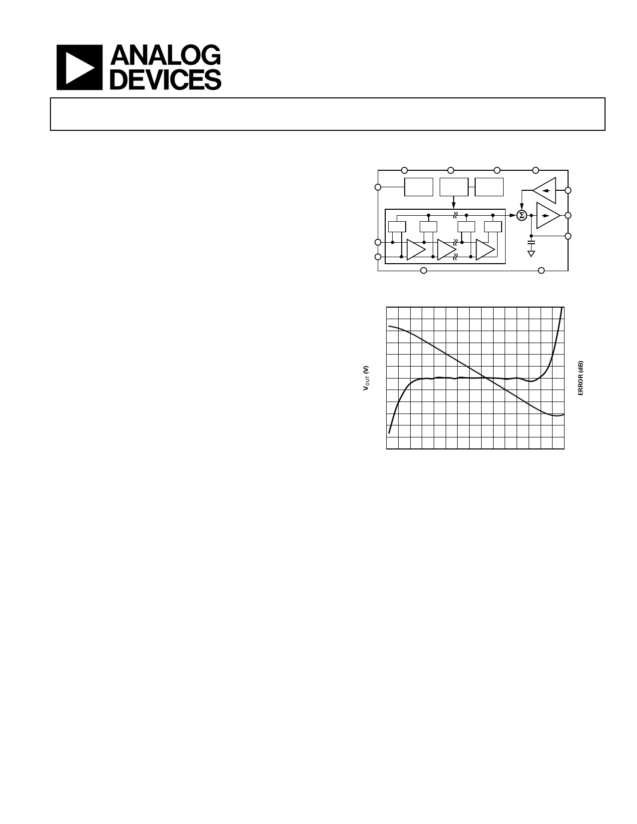
TEMP
FUNCTIONAL BLOCK DIAGRAM
VPSI
ENBL
TADJ
VPSO
TEMP
SENSOR
GAIN
BIAS
SLOPE
IV
VSET
INHI
INLO
DET
DET
DET
DET
IV
VOUT
CLPF
CMIP
Figure 1.
CMOP
2.4 6
2.2 5
2.0 4
1.8 3
1.6 2
1.4 1
1.2 0
1.0 –1
0.8 –2
0.6 –3
0.4 –4
0.2 –5
0 –6
–65 –60 –55 –50 –45 –40 –35 –30 –25 –20 –15 –10 –5 0 5 10
PIN (dBm)
Figure 2. Typical Logarithmic Response and Error vs. Input Amplitude at 5.8 GHz
In this mode, the setpoint control voltage is applied to VSET.
The feedback loop through an RF amplifier is closed via VOUT,
the output of which regulates the amplifier output to a magnitude
corresponding to VSET. The AD8318 provides 0 V to 4.9 V
output capability at the VOUT pin, suitable for controller
applications. As a measurement device, Pin VOUT is externally
connected to VSET to produce an output voltage, VOUT, which
is a decreasing linear-in-dB function of the RF input signal
amplitude.
The logarithmic slope is nominally −25 mV/dB but can be
adjusted by scaling the feedback voltage from VOUT to the
VSET interface. The intercept is 20 dBm (re: 50 Ω, CW input)
using the INHI input. These parameters are very stable against
supply and temperature variations.
The AD8318 is fabricated on a SiGe bipolar IC process and is
available in a 4 mm × 4 mm, 16-lead LFCSP for the operating
temperature range of –40oC to +85oC.
One Technology Way, P.O. Box 9106, Norwood, MA 02062-9106, U.S.A.
Tel: 781.329.4700
www.analog.com
Fax: 781.461.3113 ©2004-2007 Analog Devices, Inc. All rights reserved.
1 page 
AD8318
Parameter
Conditions
Min Typ
Max Unit
f = 3.6 GHz
RTADJ = 51 Ω
Input Impedance
119||0.7
Ω||pF
±3 dB Dynamic Range
TA = 25°C
70 dB
±1 dB Dynamic Range
TA = 25°C
58 dB
−40°C < TA < +85°C
42 dB
Maximum Input Level
±1 dB error
−2 dBm
Minimum Input Level
±1 dB error
–60 dBm
Slope
−24.3
mV/dB
Intercept
19.8 dBm
Output Voltage—High Power In
PIN = −10 dBm
0.717
V
Output Voltage—Low Power In
PIN = −40 dBm
1.46 V
Temperature Sensitivity
PIN = −10 dBm
25°C ≤ TA ≤ 85°C
0.0022
dB/°C
−40°C ≤ TA ≤ +25°C
0.004
dB/°C
f = 5.8 GHz
RTADJ = 1000 Ω
Input Impedance
33||0.59
Ω||pF
±3 dB Dynamic Range
TA = 25°C
70 dB
±1 dB Dynamic Range
TA = 25°C
57 dB
−40°C < TA < +85°C
48 dB
Maximum Input Level
±1 dB error
−1 dBm
Minimum Input Level
±1 dB error
−58 dBm
Slope
−24.3
mV/dB
Intercept
25 dBm
Output Voltage—High Power In
PIN = −10 dBm
0.86 V
Output Voltage—Low Power In
PIN = −40 dBm
1.59 V
Temperature Sensitivity
PIN = −10 dBm
25°C ≤ TA ≤ 85°C
0.0033
dB/°C
−40°C ≤ TA ≤ +25°C
0.0069
dB/°C
f = 8.0 GHz
RTADJ = 500 Ω
±3 dB Dynamic Range
TA = 25°C
60 dB
−40°C < TA < +85°C
58 dB
Maximum Input Level
±3 dB error
3 dBm
Minimum Input Level
±3 dB error
−55 dBm
Slope
−23 mV/dB
Intercept
37 dBm
Output Voltage—High Power In
PIN = −10 dBm
1.06 V
Output Voltage—Low Power In
PIN = −40 dBm
1.78 V
Temperature Sensitivity
PIN = −10 dBm
25°C ≤ TA ≤ 85°C
0.028
dB/°C
−40°C ≤ TA ≤ +25°C
−0.0085
dB/°C
OUTPUT INTERFACE
VOUT (Pin 6)
Voltage Swing
VSET = 0 V; PIN = −10 dBm, no load1
VSET = 2.1 V; PIN = −10 dBm, no load1
4.9 V
25 mV
Output Current Drive
VSET = 1.5 V; PIN = −50 dBm
60 mA
Small Signal Bandwidth
PIN = −10 dBm; from CLPF to VOUT
60 MHz
Video Bandwidth (or Envelope Bandwidth)
45 MHz
Output Noise
PIN = 2.2 GHz; −10 dBm, fNOISE = 100 kHz, CLPF = 220 pF
90
nV/√Hz
Fall Time
PIN = Off to −10 dBm, 90% to 10%
10 ns
Rise Time
PIN = −10 dBm to off, 10% to 90%
12 ns
Rev. B | Page 4 of 24
5 Page 
AD8318
j1
j0.5 j2
j0.2
0
–j0.2
0.2
8GHz
0.5
1
5.8GHz
2
0.1GHz
0.9GHz
1.9GHz
–j0.5
3.6GHz
2.2GHz
–j2
START FREQUENCY = 0.1GHz
STOP FREQUENCY = 8GHz
–j1
Figure 16. Input Impedance vs. Frequency; No Termination Resistor on
INHI, ZO = 50 Ω
0.07
0.06
0.05
0.04
DECREASING VENBL
0.03
INCREASING VENBL
0.02
0.01
0
1.4 1.5 1.6 1.7
VENBL (V)
Figure 17. Supply Current vs. Enable Voltage
1.8
VOUT
200mV/VERTICAL
DIVISION
GND
PULSED RF INPUT 0.1GHz,
–10dBm
20ns PER HORIZONTAL DIVISION
Figure 18. VOUT Pulse Response Time; Pulsed RF Input 0.1 GHz, –10 dBm;
CLPF = Open
10k
RF OFF
1k
–60dBm
–40dBm
–20dBm
100
–10dBm
0dBm
10
1
3 10 30 100 300 1k 3k 10k
FREQUENCY (kHz)
Figure 19. Noise Spectral Density of Output; CLPF = Open
1k
100
10
1
3 10 30 100 300 1k 3k 10k
FREQUENCY (kHz)
Figure 20. Noise Spectral Density of Output Buffer (from CLPF to VOUT);
CLPF = 0.1 μF
2.2 2.0
2.0 1.6
1.8 1.2
1.6 0.8
1.4 0.4
1.2 0
1.0 –0.4
0.8 –0.8
0.6 –1.2
0.4 –1.6
0.2 –2.0
–65 –55 –45 –35 –25 –15 –5 5 15
PIN (dBm)
Figure 21. Output Voltage Stability vs. Supply Voltage at 1.9 GHz
When VP Varies by 10%, Multiple Devices
Rev. B | Page 10 of 24
11 Page | ||
| Páginas | Total 25 Páginas | |
| PDF Descargar | [ Datasheet AD8318.PDF ] | |
Hoja de datos destacado
| Número de pieza | Descripción | Fabricantes |
| AD831 | Low Distortion Mixer | Analog Devices |
| AD8310 | 95 dB Logarithmic Amplifier | Analog Devices |
| AD8311 | 50 dB GSM PA Controller | Analog Devices |
| AD8312 | RF Detector | Analog Devices |
| Número de pieza | Descripción | Fabricantes |
| SLA6805M | High Voltage 3 phase Motor Driver IC. |
Sanken |
| SDC1742 | 12- and 14-Bit Hybrid Synchro / Resolver-to-Digital Converters. |
Analog Devices |
|
DataSheet.es es una pagina web que funciona como un repositorio de manuales o hoja de datos de muchos de los productos más populares, |
| DataSheet.es | 2020 | Privacy Policy | Contacto | Buscar |