|
|
|
PDF J308 Data sheet ( Hoja de datos )
| Número de pieza | J308 | |
| Descripción | (J308 / J309) JFET VHF/UHF AMPLIFIERS | |
| Fabricantes | Motorola Semiconductors | |
| Logotipo | ||
Hay una vista previa y un enlace de descarga de J308 (archivo pdf) en la parte inferior de esta página. Total 8 Páginas | ||
|
No Preview Available !
www.DataSheet4U.com
MOTOROLA
SEMICONDUCTOR TECHNICAL DATA
Order this document
by J308/D
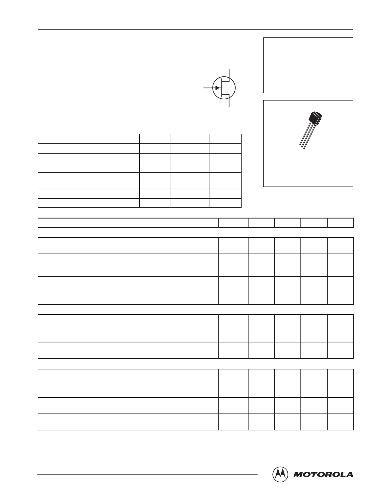
JFET VHF/UHF Amplifiers
N–Channel — Depletion
3
GATE
1 DRAIN
J308
J309
J310
Motorola Preferred Devices
2 SOURCE
MAXIMUM RATINGS
Rating
Symbol
Value
Unit
Drain – Source Voltage
Gate–Source Voltage
Forward Gate Current
Total Device Dissipation @ TA = 25°C
Derate above 25°C
VDS
VGS
IGF
PD
25 Vdc
25 Vdc
10 mAdc
350 mW
2.8 mW/°C
Junction Temperature Range
TJ – 65 to +125
Storage Temperature Range
Tstg – 65 to +150
ELECTRICAL CHARACTERISTICS (TA = 25°C unless otherwise noted)
Characteristic
°C
°C
Symbol
OFF CHARACTERISTICS
Gate – Source Breakdown Voltage
(IG = –1.0 µAdc, VDS = 0)
V(BR)GSS
Gate Reverse Current
(VGS = –15 Vdc, VDS = 0, TA = 25°C)
(VGS = –15 Vdc, VDS = 0, TA = +125°C)
Gate Source Cutoff Voltage
(VDS = 10 Vdc, ID = 1.0 nAdc)
J308
J309
J310
IGSS
VGS(off)
ON CHARACTERISTICS
Zero – Gate –Voltage Drain Current(1)
(VDS = 10 Vdc, VGS = 0)
J308
J309
J310
IDSS
Gate–Source Forward Voltage
(VDS = 0, IG = 1.0 mAdc)
VGS(f)
SMALL– SIGNAL CHARACTERISTICS
Common–Source Input Conductance
(VDS = 10 Vdc, ID = 10 mAdc, f = 100 MHz)
J308
J309
J310
Re(yis)
Common–Source Output Conductance
(VDS = 10 Vdc, ID = 10 mAdc, f = 100 MHz)
Re(yos)
Common–Gate Power Gain
(VDS = 10 Vdc, ID = 10 mAdc, f = 100 MHz)
v v1. Pulse Test: Pulse Width 300 µs, Duty Cycle 3.0%.
Gpg
Min
– 25
—
—
– 1.0
– 1.0
– 2.0
12
12
24
—
—
—
—
—
—
1
2
3
CASE 29–04, STYLE 5
TO–92 (TO–226AA)
Typ Max Unit
— — Vdc
— –1.0 nAdc
— –1.0 µAdc
Vdc
— – 6.5
— – 4.0
— – 6.5
mAdc
— 60
— 30
— 60
— 1.0 Vdc
mmhos
0.7 —
0.7 —
0.5 —
0.25 — mmhos
16 — dB
Motorola Small–Signal Transistors, FETs and Diodes Device Data
© Motorola, Inc. 1997
1
1 page 
C1
INPUT L1
RS = 50 Ω
C2
L2
VS
S
G
C3
U310
D
C4
SHIELD
C6
L3 OUTPUT
RL = 50 Ω
C5
L4
VD
J308 J309 J310
BW (3 dB) – 36.5 MHz
ID – 10 mAdc
VDS – 20 Vdc
Device case grounded
IM test tones – f1 = 449.5 MHz, f2 = 450.5 MHz
C1 = 1–10 pF Johanson Air variable trimmer.
C2, C5 = 100 pF feed thru button capacitor.
C3, C4, C6 = 0.5–6 pF Johanson Air variable
trimmer.
L1 = 1/8″ x 1/32″ x 1–5/8″ copper bar.
L2, L4 = Ferroxcube Vk200 choke.
L3 = 1/8″ x 1/32″ x 1–7/8″ copper bar.
Figure 12. 450 MHz IMD Evaluation Amplifier
Amplifier power gain and IMD products are a function of the load impedance. For the amplifier design shown above with C4 and
C6 adjusted to reflect a load to the drain resulting in a nominal power gain of 9 dB, the 3rd order intercept point (IP) value is
29 dBm. Adjusting C4, C6 to provide larger load values will result in higher gain, smaller bandwidth and lower IP values. For
example, a nominal gain of 13 dB can be achieved with an intercept point of 19 dBm.
+40
U310 JFET
+20 VDS = 20 Vdc
ID = 10 mAdc
0 F1 = 449.5 MHz
F2 = 450.5 MHz
–20
3RD ORDER INTERCEPT POINT
FUNDAMENTAL OUTPUT
–40
–60
–80
3RD ORDER IMD OUTPUT
–100
–120
–120 –100 –80 –60 –40 –20
INPUT POWER PER TONE (dBm)
0
+20
Example of intercept point plot use:
Assume two in–band signals of –20 dBm at the amplifier input.
They will result in a 3rd order IMD signal at the output of
–90 dBm. Also, each signal level at the output will be
–11 dBm, showing an amplifier gain of 9.0 dB and an
intermodulation ratio (IMR) capability of 79 dB. The gain and
IMR values apply only for signal levels below comparison.
Figure 13. Two Tone 3rd Order Intercept Point
Motorola Small–Signal Transistors, FETs and Diodes Device Data
5
5 Page | ||
| Páginas | Total 8 Páginas | |
| PDF Descargar | [ Datasheet J308.PDF ] | |
Hoja de datos destacado
| Número de pieza | Descripción | Fabricantes |
| J300 | SFET RF/VHF/ UHF/ Amplitiers | Fairchild Semiconductor |
| J300 | JFET HIGH FREQUENCY AMPLIFIER | Motorola Semiconductors |
| J300 | Trans JFET N-CH 3-Pin TO-92 Bulk | New Jersey Semiconductor |
| J3006G21D | PULSEJACKTM Surface Mount 1x1 | PULSE |
| Número de pieza | Descripción | Fabricantes |
| SLA6805M | High Voltage 3 phase Motor Driver IC. |
Sanken |
| SDC1742 | 12- and 14-Bit Hybrid Synchro / Resolver-to-Digital Converters. |
Analog Devices |
|
DataSheet.es es una pagina web que funciona como un repositorio de manuales o hoja de datos de muchos de los productos más populares, |
| DataSheet.es | 2020 | Privacy Policy | Contacto | Buscar |