|
|
PDF ZL49030 Data sheet ( Hoja de datos )
| Número de pieza | ZL49030 | |
| Descripción | (ZL49010 - ZL49031) Wide Dynamic Range DTMF Receiver | |
| Fabricantes | Zarlink Semiconductor | |
| Logotipo | ||
Hay una vista previa y un enlace de descarga de ZL49030 (archivo pdf) en la parte inferior de esta página. Total 14 Páginas | ||
|
No Preview Available !
www.DataSheet4U.com
ZL49010/1, ZL49020/1, ZL49030/1
Wide Dynamic Range DTMF Receiver
Data Sheet
Features
• Wide dynamic range (50dB) DTMF Receiver
• Call progress (CP) detection via cadence
indication
• 4-bit synchronous serial data output
• Software controlled guard time for ZL490x0
• Internal guard time circuitry for ZL490x1
• Powerdown option (ZL4901x & ZL4903x)
• 3.579MHz crystal or ceramic resonator (ZL4903x
and ZL4902x)
• External clock input (ZL4901x)
• Guarantees non-detection of spurious tones
Applications
• Integrated telephone answering machine
• End-to-end signalling
• Fax Machines
Description
The ZL490xx is a family of high performance DTMF
receivers which decode all 16 tone pairs into a 4-bit
binary code. These devices incorporate an AGC for
wide dynamic range and are suitable for end-to-end
signalling. The ZL490x0 provides an early steering
(ESt) logic output to indicate the detection of a DTMF
September 2003
Ordering Information
ZL49010DAA
ZL49011DAA
ZL49020DAA
ZL49021DAA
ZL49030DCA
ZL49030DCB
ZL49030DDA
ZL49030DDB
ZL49031DCA
ZL49031DCB
ZL49031DDA
ZL49031DDB
8 Pin PDIP Tubes
8 Pin PDIP Tubes
8 Pin PDIP Tubes
8 Pin PDIP Tubes
18 Pin SOIC Tubes
18 Pin SOIC Tape & Reel
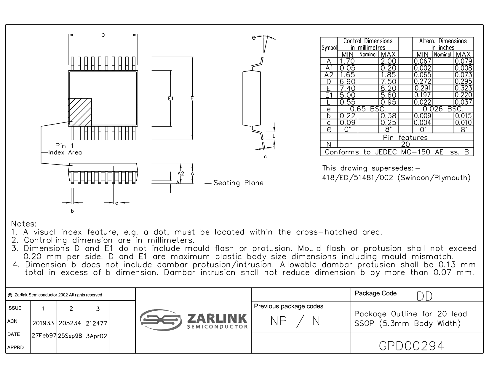
20 Pin SSOP Tubes
20 Pin SSOP Tape & Reel
18 Pin SOIC Tubes
18 Pin SOIC Tape & Reel
20 Pin SSOP Tubes
20 Pin SSOP Tape & Reel
-40°C to +85°C
signal and requires external software guard time to
validate the DTMF digit. The ZL490x1, with preset
internal guard times, uses a delay steering (DStD)
logic output to indicate the detection of a valid DTMF
digit. The 4-bit DTMF binary digit can be clocked out
synchronously at the serial data (SD) output. The SD
pin is multiplexed with call progress detector output. In
the presence of supervisory tones, the call progress
1
PWDN
VDD
VSS
Voltage
Bias Circuit
AGC
Anti-
alias
Filter
Dial
Tone
Filter
2
OSC2
OSC1
(CLK)
Oscillator
and
Clock
Circuit
To All Chip Clocks
1. ZL49010/1 and ZL49030/1 only.
2. ZL49020/1 and ZL49030/1 only.
3. ZL490x1 only.
High
Group
Filter
Low
Group
Filter
Steering
Circuit
Digital
Detector
Algorithm
Code
Converter
and
Latch
Energy
Detection
Figure 1 - Functional Block Diagram
Digital
Guard
Time3
Parallel to
Serial
Converter
& Latch
Mux
ESt
or
DStD
ACK
SD
1
Zarlink Semiconductor Inc.
Zarlink, ZL and the Zarlink Semiconductor logo are trademarks of Zarlink Semiconductor Inc.
Copyright 2003, Zarlink Semiconductor Inc. All Rights Reserved.
1 page 
ZL49010/1, ZL49020/1, ZL49030/1
FLOW
FHIGH DIGIT b3 b2 b1
941 1336 0 1 0 1
941 1209
* 101
941 1477 # 1 1 0
697 1633 A 1 1 0
770 1633 B 1 1 1
852 1633 C 1 1 1
941 1633 D 0 0 0
0= LOGIC LOW, 1= LOGIC HIGH
Note: b0=LSB of decoded DTMF digit and shifted out first.
Table 2 - Serial Decode Bit Table (continued)
b0
0
1
0
1
0
1
0
Data Sheet
ACK (input)
PWDN (input)
ESt/DStD (output)
SD (output)
low low Refer to Fig. 4 for
timing waveforms
low high+ low
high low low
high high
Note: + =enters powerdown mode on the rising edge.
undefined
Refer to Fig. 4 for
timing waveforms
low
undefined
undefined
Table 3 - Powerdown Mode
ZL4901x/4903x
status
normal operation
powerdown mode
undefined
undefined
Frequency 1 (Hz)
350
425
400
480
440
480
440
480
Frequency 2 (Hz)
440
---
---
620
---
620
480
620
On/Off
continuous
continuous
continuous
0.5s/0.5s
0.5s/0.5s
0.25s/0.25s
2.0s/4.0s
0.25s/0.25s
Description
North American Dial Tones
European Dial Tones
Far East Dial Tones
North American Line Busy
Japanese Line Busy
North American Reorder Tones
North American Audible Ringing
North American Reorder Tones
Table 4 - Call Progress Tones
Oscillator
The ZL4902x/4903x can be used in both external clock or two pin oscillator mode. In two pin oscillator mode, the
oscillator circuit is completed by connecting either a 3.579MHz crystal or ceramic resonator across OSC1 and
OSC2 pins. It is also possible to configure a number of these devices (4 maximum) employing only a single
oscillator crystal. The OSC2 output of the first device in the chain is connected to the OSC1 input of the next
device. Subsequent devices are connected similarily. The oscillator circuit can also be driven by an 3.579MHz
external clock applied on pin OSC 1. The OSC2 pin should be left open.
For ZL4901x devices, the CLK input is driven directly by an 3.579MHz external digital clock.
5
Zarlink Semiconductor Inc.
5 Page 
11 Page | ||
| Páginas | Total 14 Páginas | |
| PDF Descargar | [ Datasheet ZL49030.PDF ] | |
Hoja de datos destacado
| Número de pieza | Descripción | Fabricantes |
| ZL49030 | (ZL49010 - ZL49031) Wide Dynamic Range DTMF Receiver | Zarlink Semiconductor |
| ZL49031 | (ZL49010 - ZL49031) Wide Dynamic Range DTMF Receiver | Zarlink Semiconductor |
| Número de pieza | Descripción | Fabricantes |
| SLA6805M | High Voltage 3 phase Motor Driver IC. |
Sanken |
| SDC1742 | 12- and 14-Bit Hybrid Synchro / Resolver-to-Digital Converters. |
Analog Devices |
|
DataSheet.es es una pagina web que funciona como un repositorio de manuales o hoja de datos de muchos de los productos más populares, |
| DataSheet.es | 2020 | Privacy Policy | Contacto | Buscar |
