|
|
|
PDF ZL30416 Data sheet ( Hoja de datos )
| Número de pieza | ZL30416 | |
| Descripción | SONET/SDH Clock Multiplier PLL | |
| Fabricantes | Zarlink Semiconductor | |
| Logotipo | ||
Hay una vista previa y un enlace de descarga de ZL30416 (archivo pdf) en la parte inferior de esta página. Total 22 Páginas | ||
|
No Preview Available !
www.DataSheet4U.com
ZL30416
SONET/SDH Clock Multiplier PLL
Data Sheet
Features
• Low jitter clock outputs suitable for OC-192, OC-
48, OC-12, OC-3 and OC-1 SONET applications
as defined in Telcordia GR-253-CORE
• Low jitter clock outputs suitable for STM-64, STM-
16, STM-4 and STM-1 applications as defined in
ITU-T G.813
• Provides one differential LVPECL output clock
selectable to 19.44, 38.88, 77.76, 155.52 or
622.08 MHz
• Provides a single-ended CMOS output clock at
19.44 MHz
• Accepts a single-ended CMOS reference at
19.44 MHz or a differential LVDS, LVPECL or
CML reference at 19.44 or 77.76 MHz
• Provides a LOCK indication
• 8 mm x 8 mm CABGA package
• 3.3 V supply
Applications
• SONET/SDH line cards
November 2004
Ordering Information
ZL30416GGG
64 Ball CABGA
-40°C to +85°C
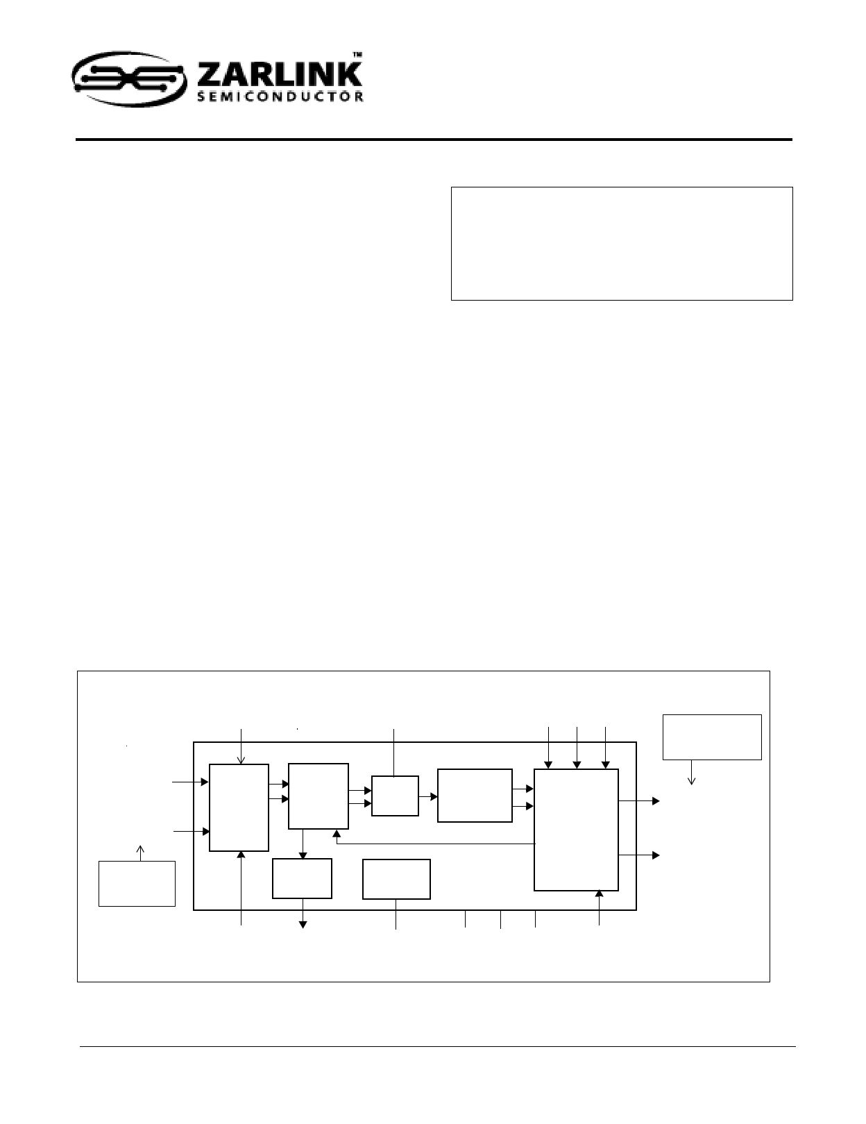
Description
The ZL30416 is an Analog Phase-Locked Loop (APLL)
designed to provide jitter attenuation and rate
conversion for SDH (Synchronous Digital Hierarchy)
and SONET (Synchronous Optical Network)
networking equipment. The ZL30416 generates low
jitter output clocks suitable for Telcordia GR-253-
CORE OC-192, OC-48, OC-12, OC-3, and OC-1 and
ITU-T G.813 STM-64, STM-16, STM-4 and STM-1
applications.
The ZL30416 accepts a CMOS compatible reference
at 19.44 MHz or a differential LVDS, LVPECL or CML
reference at 19.44 or 77.76 MHz and generates a
differential LVPECL output clock selectable to 19.44,
38.88, 77.76, 155.52 or 622.08 MHz and a single-
ended CMOS clock at 19.44 MHz. The ZL30416
provides a lock indication.
REF_SEL
LPF
FS3 FS2 FS1
C19i
REFinP/N
C19i or C77i
CML, LVDS,
LVPECL input
Reference
Selection
MUX
Frequency
& Phase
Detector
State
Machine
Loop
Filter
VCO
19.44 MHz and 77.76 MHz
Reference
and
Bias Circuit
Frequency
Dividers
and
Clock
Drivers
REF_FREQ LOCK
BIAS
VCC GND VDD C19oEN
C19o, C38o, C77o,
C155o, C622o,
LVPECL output
OC-CLKoP/N
C19o
Figure 1 - Functional Block Diagram
1
Zarlink Semiconductor Inc.
Zarlink, ZL and the Zarlink Semiconductor logo are trademarks of Zarlink Semiconductor Inc.
Copyright 2004, Zarlink Semiconductor Inc. All Rights Reserved.
1 page 
ZL30416
Data Sheet
2.2 Frequency/Phase Detector
The Frequency/Phase Detector compares the frequency/phase of the input reference signal with the feedback
signal from the Frequency Divider circuit and provides an error signal equal to the frequency/phase
difference between the two. This error signal is passed to the Loop Filter circuit.
2.3 Lock Indicator
The ZL30416 has a built-in LOCK detector that measures frequency difference between input reference clock C19i
and the VCO frequency. When the VCO frequency is less than ±300 ppm apart from the input reference frequency
then the LOCK output is set high. The LOCK output is pulled low if the frequency difference exceeds ±1000 ppm.
2.4 Loop Filter
The Loop Filter is a low-pass filter. This low-pass filter eliminates high frequency spectral components from a phase
error signal produced by the Phase Detector. This ensures low output jitter that meets network jitter requirements.
The corner frequency of the Loop Filter is configurable with an external capacitor and resistor connected to the LPF
ball and ground as shown in Figure 3.
Frequency
and Phase
Detector
VCO
ZL30416
Loop
Filter
LPF
RF
CF
RF=8.2 kΩ, CF=470 nF
fTYP=14.4 kHz
Figure 3 - Loop Filter Elements
2.5 VCO
The voltage-controlled oscillator (VCO) receives the filtered error signal from the Loop Filter and based on the
voltage of the error signal generates a primary frequency. The VCO output is connected to the "Frequency Dividers
and Clock Drivers" block that divides VCO frequency and buffer generated clocks.
5
Zarlink Semiconductor Inc.
5 Page 
ZL30416
Data Sheet
4.3 Power supply and BIAS Circuit Filtering Recommendations
Figure 9 presents a complete filtering arrangement that is recommended for applications requiring maximum jitter
performance. The level of required filtering is subject to further optimization and simplification. Please check
Zarlink’s web site for updates.
Ferrite Bead
0.1 uF 0.1 uF
10 uF
12345678
1
+3.3 V Power Rail
4.7 Ω
A
33 uF
220 Ω
B
0.1 uF 0.1 uF
33 uF
C
D
33 uF 0.1 uF
E
F
G
H
NC NC
NC OC-CLKoP OC-CLKoN GND NC
NC
NC NC VCC1 GND NC GND GND VCC
GND VCC2 GND GND GND NC VDD GND
BIAS LPF NC GND VCC VCC GND GND
LOCK NC
NC FS2
VCC VDD
NC REFinN
NC NC REF_FREQ C19oEN C19i C19o GND REFinP
GND VDD REF_SEL FS3 GND GND VDD VDD
NC NC NC VDD FS1 VDD GND GND
0.1 uF 0.1 uF
0.1 uF 0.1 uF
0.1 uF 0.1 uF
0.1 uF
0.1 uF 0.1 uF 0.1 uF 0.1 uF
Notes:
1. All the ground pins (GND) are connected to the same ground plane.
2. Select Ferrite Bead with IDC > 400 mA and RDC in a range from 0.10 Ω to 0.15 Ω.
Figure 9 - Power Supply and BIAS Circuit Filtering
11
Zarlink Semiconductor Inc.
11 Page | ||
| Páginas | Total 22 Páginas | |
| PDF Descargar | [ Datasheet ZL30416.PDF ] | |
Hoja de datos destacado
| Número de pieza | Descripción | Fabricantes |
| ZL30410 | Multi-service Line Card PLL | Zarlink Semiconductor |
| ZL30414 | SONET/SDH Clock Multiplier PLL | Zarlink Semiconductor |
| ZL30415 | SONET/SDH Clock Multiplier PLL | Zarlink Semiconductor |
| ZL30416 | SONET/SDH Clock Multiplier PLL | Zarlink Semiconductor |
| Número de pieza | Descripción | Fabricantes |
| SLA6805M | High Voltage 3 phase Motor Driver IC. |
Sanken |
| SDC1742 | 12- and 14-Bit Hybrid Synchro / Resolver-to-Digital Converters. |
Analog Devices |
|
DataSheet.es es una pagina web que funciona como un repositorio de manuales o hoja de datos de muchos de los productos más populares, |
| DataSheet.es | 2020 | Privacy Policy | Contacto | Buscar |