|
|
|
PDF MM1389 Data sheet ( Hoja de datos )
| Número de pieza | MM1389 | |
| Descripción | Pedestal Clamp 2-Input 1-Output 3-Circuit Video Switch | |
| Fabricantes | Mitsumi Electronics | |
| Logotipo | ||
Hay una vista previa y un enlace de descarga de MM1389 (archivo pdf) en la parte inferior de esta página. Total 7 Páginas | ||
|
No Preview Available !
www.DataSheet4U.com
MITSUMI
Pedestal Clamp 2-Input 1-Output 3-Circuit Video Switch MM1389
Pedestal Clamp 2-Input 1-Output 3-Circuit Video Switch
Monolithic IC MM1389
April 1, 1997
Outline
This is a video switch IC developed for use in video cameras, with 2-input and 1-output circuits. It has
pedestal clamp input, making it ideal for RGB and video signal switching,
Features
1. Pedestal clamp input
2. Low current consumption
3. Frequency response
4. Operating power supply voltage
12mA typ.(VCC5V)
10MHz typ. 0dB
4.5~12V
Package
SOP-16B (MM1389XF)
Applications
1. TV
2. VCR
3. Other video equipment
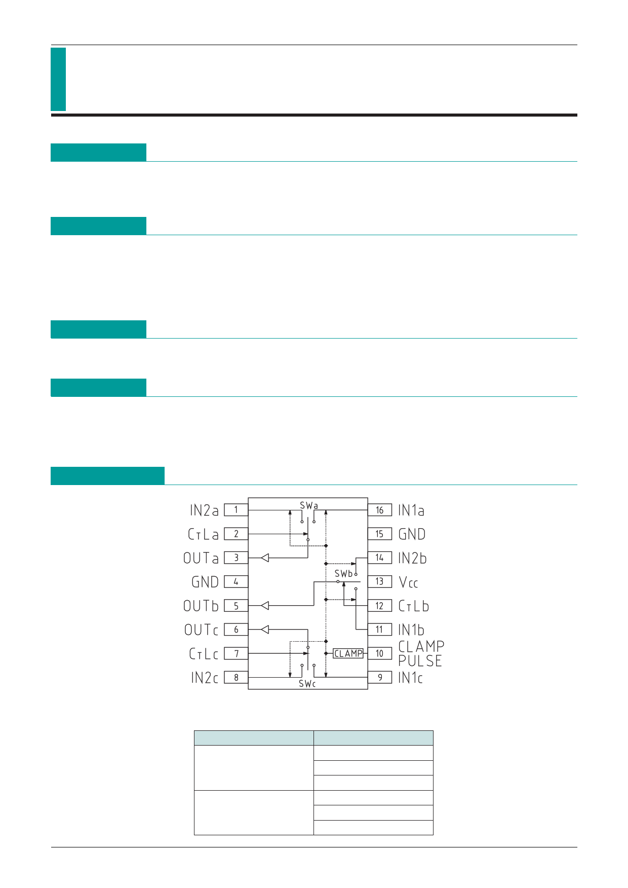
Block Diagram
Control input truth table
SW OUT
IN2a
L IN2b
IN2c
IN1a
H IN1b
IN1c
1 page 
MITSUMI
Pedestal Clamp 2-Input 1-Output 3-Circuit Video Switch MM1389
(Except where noted otherwise, VCC=5.0V, VC1=VCC, VC2=0V, PULSE=VCC, C1~C6=0.1µF, impress VB=3.5V when S9 is 2)
Item
Consumption current
Symbol
ID
Voltage gain
GV
Frequency characteristic
FC
Dynamic range 1, 2
VD1
VD2
Crosstalk
CT
Switch input voltage H, L
VIH
VIL
Clamp pin input voltage H, L
VCTH
VCTL
Measurement conditions
Notes
Connect a DC ammeter to the VCC pin and measure. The
ammeter is shorted for subsequent measurements.
Input a 2.0VP-P, 100kHz sine wave to SG, and obtain
GV from the following formula given TP1 voltage as V1 f=100kHz
and TP3 voltage as V2.
V=2.0VP-P
GV=20Log (V2/V1) dB
For the above GV measurement, given TP3 voltage for
10MHz as V3, FC is obtained from the following formula.
FC=20Log (V3/V2) dB
10MHz/100kHz
V=2.0VP-P
Input a video signal to SG and a 5VP-P clamp pulse to PULSE.
Given input amplitude on the positive side of clamp level VC
as VD1IN, and output amplitude as VD1OUT and negative side
input amplitude as VD2IN, and output amplitude as VD2OUT,
VD2 is obtained from the following formula.
VD1 : 20Log (VD1OUT/VD1IN) <= VD1IN for-1dB
VD2 : 20Log (VD2OUT/VD2IN) <= VD2IN for-1dB
Input a 2.0VP-P, 4.43MHz sine wave to SG, and given
TP1 voltage as V4 and TP3 voltage as V5, CT is
f=4.43MHz
obtained from the following formula.
V=2.0VP-P
CT=20Log (V5/V4) dB
Make S10, S12 and S14 1, and S11, S13 and S15 2.
Input a 2.0VP-P, 100kHz sine wave to SG, and raise
gradually from VC1=0V. TP4 voltage when the SG
signal appears on TP2 is VIN. Next, reverse S10~S15
settings and lower gradually from VC1=VCC. TP4
voltage when the SG signal appears on TP2 is VIL.
Impress 4V on VB and raise gradually from
PULSE=0V. TP11 voltage when less than 2.0V appears
on TP2 is VCTH. Lower from PULSE=VCC, and TP11
voltage when more than 2.2V appears on TP2 is VCTL.
5 Page | ||
| Páginas | Total 7 Páginas | |
| PDF Descargar | [ Datasheet MM1389.PDF ] | |
Hoja de datos destacado
| Número de pieza | Descripción | Fabricantes |
| MM1381 | RGB Video Amplifier with OSD Input | MITSUMI |
| MM1382 | RGB Video Amplifier with OSD Input | MITSUMI |
| MM1383 | RGB Video Amplifier with OSD Input | MITSUMI |
| MM1385 | Microminiature Low-Power Consumption Low-Saturation Regulator | Mitsumi Electronics |
| Número de pieza | Descripción | Fabricantes |
| SLA6805M | High Voltage 3 phase Motor Driver IC. |
Sanken |
| SDC1742 | 12- and 14-Bit Hybrid Synchro / Resolver-to-Digital Converters. |
Analog Devices |
|
DataSheet.es es una pagina web que funciona como un repositorio de manuales o hoja de datos de muchos de los productos más populares, |
| DataSheet.es | 2020 | Privacy Policy | Contacto | Buscar |