|
|
|
PDF AD8045 Data sheet ( Hoja de datos )
| Número de pieza | AD8045 | |
| Descripción | High Speed Op Amp | |
| Fabricantes | Analog Devices | |
| Logotipo | ||
Hay una vista previa y un enlace de descarga de AD8045 (archivo pdf) en la parte inferior de esta página. Total 25 Páginas | ||
|
No Preview Available !
Data Sheet
FEATURES
Ultralow distortion
SFDR
−101 dBc at 5 MHz
−90 dBc at 20 MHz
−63 dBc at 70 MHz
Third-order intercept
43 dBm at 10 MHz
Low noise
3 nV/√Hz
3 pA/√Hz
High speed
1 GHz, −3 dB bandwidth (G = +1)
1350 V/µs slew rate
7.5 ns settling time to 0.1%
Standard and low distortion pinout
Supply current: 15 mA
Offset voltage: 1.0 mV max
Wide supply voltage range: 3.3 V to 12 V
APPLICATIONS
Instrumentation
IF and baseband amplifiers
Active filters
ADC drivers
DAC buffers
GENERAL DESCRIPTION
The AD8045 is a unity-gain stable voltage feedback amplifier
with ultralow distortion, low noise, and high slew rate. With a
spurious-free dynamic range of −90 dBc at 20 MHz, the AD8045 is
an ideal solution in a variety of applications, including ultrasound,
automated test equipment (ATE), active filters, and analog-to-
digital converter (ADC) drivers. The Analog Devices, Inc.,
proprietary next generation XFCB process and innovative
architecture enable such high performance amplifiers.
The AD8045 features a low distortion pinout for the LFCSP,
which improves second harmonic distortion and simplifies the
layout of the circuit board.
The AD8045 has a 1 GHz bandwidth, a 1350 V/µs slew rate, and
settles to 0.1% in 7.5 ns. With a wide supply voltage range (3.3 V
to 12 V) and a low offset voltage (200 µV), the AD8045 is an
ideal candidate for systems that require high dynamic range,
precision, and high speed.
The AD8045 amplifier is available in a 3 mm × 3 mm LFCSP
and the standard 8-lead SOIC. Both packages feature an exposed
Rev. B
Document Feedback
Information furnished by Analog Devices is believed to be accurate and reliable. However, no
responsibility is assumed by Analog Devices for its use, nor for any infringements of patents or other
rights of third parties that may result from its use. Specifications subject to change without notice. No
license is granted by implication or otherwise under any patent or patent rights of Analog Devices.
Trademarksandregisteredtrademarksarethepropertyoftheirrespectiveowners.
3 nV/√Hz, Ultralow Distortion,
High Speed Op Amp
AD8045
CONNECTION DIAGRAMS
AD8045
TOP VIEW
(Not to Scale)
NIC 1
FEEDBACK 2
8 +VS
7 OUTPUT
–IN 3
6 NIC
+IN 4
5 –VS
NOTES
1. NIC = NO INTERNAL CONNECTION.
Figure 1. 8-Lead AD8045 LFCSP (CP-8)
AD8045
TOP VIEW
(Not to Scale)
FEEDBACK 1
–IN 2
+IN 3
–VS 4
8 NIC
7 +VS
6 OUTPUT
5 NIC
NOTES
1. NIC = NO INTERNAL CONNECTION.
Figure 2. 8-Lead AD8045 SOIC/EP (RD-8)
paddle that provides a low thermal resistance path to the
printed circuit board (PCB). This enables more efficient heat
transfer and increases reliability. The AD8045 works over the
extended industrial temperature range (−40°C to +125°C).
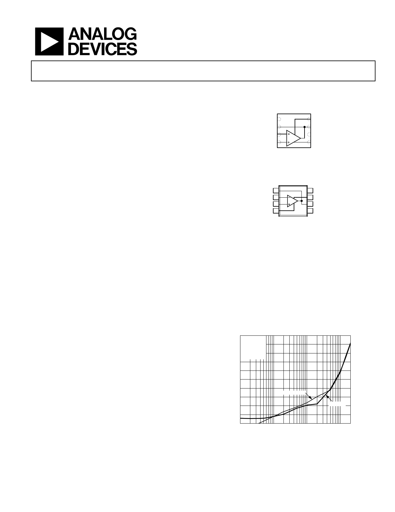
–20
G = +1
–30 VS = ±5V
VOUT = 2V p-p
–40 RL = 1kΩ
RS = 100Ω
–50
–60
–70
–80
–90
–100
HD3 LFCSP
HD2 LFCSP
–110
–120
0.1 1 10 100
FREQUENCY (MHz)
Figure 3. Harmonic Distortion vs. Frequency for Various Packages
One Technology Way, P.O. Box 9106, Norwood, MA 02062-9106, U.S.A.
Tel: 781.329.4700 ©2004–2016 Analog Devices, Inc. All rights reserved.
Technical Support
www.analog.com
1 page 
AD8045
Data Sheet
SPECIFICATIONS WITH +5 V SUPPLY
TA = 25°C, G = +1, RS = 100 Ω, RL = 1 kΩ to midsupply, unless otherwise noted. Exposed paddle must be floating or connected to −VS.
Table 2.
Parameter
DYNAMIC PERFORMANCE
–3 dB Bandwidth
Bandwidth for 0.1 dB Flatness
Slew Rate
Settling Time to 0.1%
NOISE/HARMONIC PERFORMANCE
Harmonic Distortion (dBc) HD2/HD3
Input Voltage Noise
Input Current Noise
Differential Gain Error
Differential Phase Error
DC PERFORMANCE
Input Offset Voltage
Input Offset Voltage Drift
Input Bias Current
Input Bias Current Drift
Input Bias Offset Current
Open-Loop Gain
INPUT CHARACTERISTICS
Input Resistance
Input Capacitance
Input Common-Mode Voltage Range
Common-Mode Rejection
OUTPUT CHARACTERISTICS
Output Overdrive Recovery Time
Output Voltage Swing
Output Current
Short-Circuit Current
Capacitive Load Drive
POWER SUPPLY
Operating Range
Quiescent Current
Positive Power Supply Rejection
Negative Power Supply Rejection
Test Conditions/Comments
G = +1, VOUT = 0.2 V p-p
G = +1, VOUT = 2 V p-p
G = +2, VOUT = 0.2 V p-p
G = +2, VOUT = 2 V p-p, RL = 150 Ω
G = +1, VOUT = 2 V step
G = +2, VOUT = 2 V step
fC = 5 MHz, VOUT = 2 V p-p
LFCSP
SOIC
fC = 20 MHz, VOUT = 2 V p-p
LFCSP
SOIC
fC = 70 MHz, VOUT = 2 V p-p
LFCSP
SOIC
f = 100 kHz
f = 100 kHz
NTSC, G = +2, RL = 150 Ω
NTSC, G = +2, RL = 150 Ω
See Figure 54
VOUT = 2 V to 3 V
Common-mode/differential
Common-mode
VCM = 2 V to 3 V
VIN = −0.5 V to +3 V, G = +2
RL = 1 kΩ
RL = 100 Ω
Sinking/sourcing
30% overshoot, G = +2
+VS = +5 V to +6 V, −VS = 0 V
+VS = +5 V, −VS = 0 V to −1 V
Min
160
320
480
61
−78
2.2 to 3.7
2.5 to 3.5
3.3
−65
−70
Typ
900
200
395
60
1060
10
−89/−83
−92/−83
−81/−70
−83/−70
−57/−46
−57/−46
3
3
0.01
0.01
0.5
7
2
7
0.2
63
3/0.9
1.3
1.2 to 3.8
−94
10
1.1 to 4.0
1.2 to 3.8
55
70/140
15
5
15
−67
−73
Max Unit
MHz
MHz
MHz
MHz
V/µs
ns
dBc
dBc
dBc
dBc
dBc
dBc
nV/√Hz
pA/√Hz
%
Degrees
1.4 mV
µV/°C
6.6 µA
nA/°C
1.3 µA
dB
MΩ
pF
V
dB
ns
V
V
mA
mA
pF
12 V
18 mA
dB
dB
Rev. B | Page 4 of 24
5 Page 
AD8045
–40
G = +1
VS = ±5V
–50 RL = 150
RS = 100
f = 10MHz
–60
HD2 LFCSP
–70
HD2 SOIC
–80
–90
–100
HD3 SOIC AND LFCSP
–110
012345678
OUTPUT AMPLITUDE (V p-p)
Figure 25. Harmonic Distortion vs. Output Voltage for Various Packages
–40 G = –1
VS = ±5V
–50 RL = 1k
f = 10MHz
–60 SOIC AND LFCSP
–70
–80
–90
–100
HD2
HD3
–110
–120
01234567
OUTPUT VOLTAGE (V p-p)
Figure 26. Harmonic Distortion vs. Output Voltage
8
–40
G = –1
–50
VS = ±5V
RL = 150
f = 10MHz
–60
–70
HD2 SOIC
–80
HD2 LFCSP
–90
–100
HD3 SOIC AND LFCSP
–110
–120
01234567
OUTPUT VOLTAGE (V p-p)
Figure 27. Harmonic Distortion vs. Output Voltage
8
Data Sheet
–30
G = +1
VS = ±2.5
–40 VOUT = 2V p-p
RL = 1k
RS = 100
–50
–60
HD3 SOIC AND LFCSP
–70
–80
HD2 LFCSP
–90
HD2 SOIC
–100
1
10
FREQUENCY (MHz)
100
Figure 28. Harmonic Distortion vs. Frequency for Various Packages
–20
G = +1
–30
VS = ±2.5V
VOUT = 2V p-p
RL = 100
–40 RS = 100
–50
–60
HD3 SOIC AND LFCSP
–70
–80
HD2 LFCSP
–90
–100
1
HD2 SOIC
10
FREQUENCY (MHz)
100
Figure 29. Harmonic Distortion vs. Frequency for Various Packages
–20 G = –1
VS = ±2.5V
–30 VOUT = 2V p-p
RL = 1k
–40 SOIC AND LFCSP
–50
–60
HD3
–70
–80
HD2
–90
–100
0.1
1 10
FREQUENCY (MHz)
100
Figure 30. Harmonic Distortion vs. Frequency for Various Packages
Rev. B | Page 10 of 24
11 Page | ||
| Páginas | Total 25 Páginas | |
| PDF Descargar | [ Datasheet AD8045.PDF ] | |
Hoja de datos destacado
| Número de pieza | Descripción | Fabricantes |
| AD8040 | Rail-to-Rail Input/Output Amplifier | Analog Devices |
| AD8041 | Rail-to-Rail Amplifier | Analog Devices |
| AD8042 | Dual 160 MHz Rail-to-Rail Amplifier | Analog Devices |
| AD8044 | Quad 150 MHz Rail-to-Rail Amplifier | Analog Devices |
| Número de pieza | Descripción | Fabricantes |
| SLA6805M | High Voltage 3 phase Motor Driver IC. |
Sanken |
| SDC1742 | 12- and 14-Bit Hybrid Synchro / Resolver-to-Digital Converters. |
Analog Devices |
|
DataSheet.es es una pagina web que funciona como un repositorio de manuales o hoja de datos de muchos de los productos más populares, |
| DataSheet.es | 2020 | Privacy Policy | Contacto | Buscar |