|
|
|
PDF AD8000 Data sheet ( Hoja de datos )
| Número de pieza | AD8000 | |
| Descripción | Ultrahigh Speed Op Amp | |
| Fabricantes | Analog Devices | |
| Logotipo | ||
Hay una vista previa y un enlace de descarga de AD8000 (archivo pdf) en la parte inferior de esta página. Total 18 Páginas | ||
|
No Preview Available !
Data Sheet
1.5 GHz, Ultrahigh Speed Op Amp
AD8000
FEATURES
High speed
1.5 GHz, −3 dB bandwidth (G = +1)
650 MHz, full power bandwidth (G = +2, VO = 2 V p-p)
Slew rate: 4100 V/μs
0.1% settling time: 12 ns
Excellent video specifications
0.1 dB flatness: 170 MHz
Differential gain: 0.02%
Differential phase: 0.01°
Output overdrive recovery: 22 ns
Low noise: 1.6 nV/√Hz input voltage noise
Low distortion over wide bandwidth
75 dBc SFDR at 20 MHz
62 dBc SFDR at 50 MHz
Input offset voltage: 1 mV typical
High output current: 100 mA
Wide supply voltage range: 4.5 V to 12 V
Supply current: 13.5 mA
Power-down mode
APPLICATIONS
Professional video
High speed instrumentation
Video switching
IF/RF gain stage
CCD imaging
GENERAL DESCRIPTION
The AD8000 is an ultrahigh speed, high performance, current
feedback amplifier. Using Analog Devices, Inc., proprietary
eXtra Fast Complementary Bipolar (XFCB) process, the ampli-
fier can achieve a small signal bandwidth of 1.5 GHz and a slew
rate of 4100 V/μs.
The AD8000 has low spurious-free dynamic range (SFDR) of
75 dBc at 20 MHz and input voltage noise of 1.6 nV/√Hz. The
AD8000 can drive over 100 mA of load current with minimal
distortion. The amplifier can operate on +5 V to ±6 V. These
specifications make the AD8000 ideal for a variety of applica-
tions, including high speed instrumentation.
With a differential gain of 0.02%, differential phase of 0.01°, and
0.1 dB flatness out to 170 MHz, the AD8000 has excellent video
specifications, which ensure that even the most demanding
video systems maintain excellent fidelity.
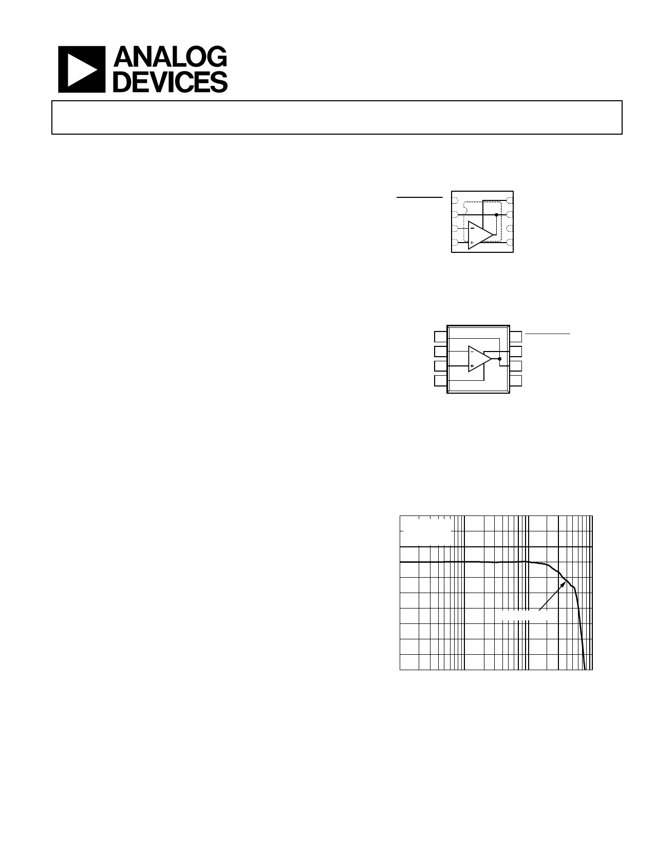
CONNECTION DIAGRAMS
AD8000
TOP VIEW
(Not to Scale)
POWER DOWN 1
FEEDBACK 2
–IN 3
+IN 4
8 +VS
7 OUTPUT
6 NC
5 –VS
NOTES
1. NC = NO CONNECT.
2. THE EXPOSED PADDLE IS CONNECTED TO GROUND.
Figure 1. 8-Lead AD8000, 3 mm × 3 mm LFCSP (CP-8-13)
AD8000
TOP VIEW
(Not to Scale)
FEEDBACK 1
8 POWER DOWN
–IN 2
+IN 3
7 +VS
6 OUTPUT
–VS 4
5 NC
NOTES
1. NC = NO CONNECT.
2. THE EXPOSED PADDLE IS CONNECTED TO GROUND.
Figure 2. 8-Lead AD8000 SOIC_N_EP (RD-8-1)
The AD8000 power-down mode reduces the supply current to
1.3 mA. The amplifier is available in a tiny 8-lead LFCSP package,
as well as in an 8-lead SOIC package. The AD8000 is rated to work
over the extended industrial temperature range (−40°C to +125°C).
A triple version of the AD8000 (AD8003) is underdevelopment.
3
VS = 5V
2 RL = 150
VOUT = 2V p-p
1
0
–1
–2
–3
G = +2, RF = 432
–4
–5
–6
–7
1 10 100
FREQUENCY (MHz)
Figure 3. Large Signal Frequency Response
1000
Rev. C
Document Feedback
Information furnished by Analog Devices is believed to be accurate and reliable. However, no re-
sponsibility is assumed by Analog Devices for its use, nor for any infringements of patents or other
rights of third parties that may result from its use. Specifications subject to change without notice. No
license is granted by implication or otherwise under any patent or patent rights of Analog Devices.
Trademarksandregisteredtrademarksarethepropertyoftheirrespectiveowners.
One Technology Way, P.O. Box 9106, Norwood, MA 02062-9106, U.S.A.
Tel: 781.329.4700 ©2005–2016 Analog Devices, Inc. All rights reserved.
Technical Support
www.analog.com
1 page 
AD8000
Data Sheet
SPECIFICATIONS WITH +5 V SUPPLY
At TA = 25°C, VS = 5 V, RL = 150 Ω, Gain = +2, RF = RG = 432 Ω, unless otherwise noted. Connect the exposed paddle to ground.
Table 2.
Parameter
DYNAMIC PERFORMANCE
−3 dB Bandwidth
Bandwidth for 0.1 dB Flatness
Slew Rate
Settling Time to 0.1%
NOISE/HARMONIC PERFORMANCE
Second/Third Harmonic
Second/Third Harmonic
Input Voltage Noise
Input Current Noise
Differential Gain Error
Differential Phase Error
DC PERFORMANCE
Input Offset Voltage
Input Offset Voltage Drift
Input Bias Current (Enabled)
Transimpedance
INPUT CHARACTERISTICS
Noninverting Input Impedance
Input Common-Mode Voltage Range
Common-Mode Rejection Ratio
Overdrive Recovery
POWER DOWN PIN
Power-Down Input Voltage
Turn-Off Time
Turn-On Time
Input Current
Enabled
Power-Down
OUTPUT CHARACTERISTICS
Output Voltage Swing
Linear Output Current
Overdrive Recovery
POWER SUPPLY
Operating Range
Quiescent Current
Quiescent Current (Power-Down)
Power Supply Rejection Ratio
Test Conditions/Comments
G = +1, VO = 0.2 V p-p
G = +2, VO = 2 V p-p
G = +10, VO = 0.2 V p-p
VO = 0.2 V p-p
VO = 2 V p-p
G = +2, VO = 2 V step
G = +2, VO = 2 V step
VO = 2 V p-p, 5 MHz, LFCSP only
VO = 2 V p-p, 20 MHz, LFCSP only
f = 100 kHz
f = 100 kHz, −IN
f = 100 kHz, +IN
NTSC, G = +2
NTSC, G = +2
+IB
−IB
VCM = ±2.5 V
G = +1, f = 1 MHz, triangle wave
Power-down
Enable
50% of power-down voltage to
10% of VOUT final, VIN = 0.3 V p-p
50% of power-down voltage to
90% of VOUT final, VIN = 0.3 V p-p
RL = 100 Ω
RL = 1 kΩ
VO = 2 V p-p, second HD < −50 dBc
G = +2, f = 100 kHz, triangle wave
−PSRR/+PSRR
Min Typ
Max Unit
980
477
328
136
136
2700
16
MHz
MHz
MHz
MHz
MHz
V/μs
ns
71/71
60/62
1.6
26
3.4
0.01
0.06
dBc
dBc
nV/√Hz
pA/√Hz
pA/√Hz
%
Degree
1.3
18
−5
−1
440 800
10
+3
+45
1500
mV
μV/°C
μA
μA
kΩ
2/3.6
MΩ/pF
1.5 to 3.6
V
−51 −52
−54 dB
60 ns
< +VS − 3.1
> +VS − 1.9
200
300
V
V
ns
ns
−1.1 +0.17
−50 −40
+1.4 μA
−30 μA
1.1 to 3.9
1 to 4.0
1.05 to 4.1
0.85 to 4.15
70
65
V
V
mA
ns
4.5
11
0.7
−55/−60
12
0.95
−57/−62
12 V
13 mA
1.25 mA
dB
Rev. C | Page 4 of 17
5 Page 
AD8000
–40
VS = 5V
–50
VOUT = 2V p-p
G = –1
RL = 1k
–60 LFCSP
–70
SECOND HD
–80
THIRD HD
–90
–100
–110
–120
1
10
FREQUENCY (MHz)
Figure 29. Harmonic Distortion vs. Frequency
1k
VS = 5V
VIN = 0.2V p-p
RF = 432
100 LFCSP
100
10
1
G = +1
0.1 OR G = +2
0.01
0.1
1
10 100
FREQUENCY (MHz)
Figure 30. Output Impedance vs. Frequency
1000
2.65
G = +1
2.60
2.55
G = +2
2.50
2.45
2.40
2.35
0
VS = 5V
RF = 432
RS = 0
RL = 100
5 10 15 20 25 30 35 40 45 50
TIME (ns)
Figure 31. Small Signal Transient Response
Data Sheet
–10
–15
VS = 5V
VIN = 2V p-p
–20 RL = 100
G = +1
–25 RF = 432
–30
–35
–40
–45
–50
–55
–60
–65
–70
–75
0.1
–PSRR
1
+PSRR
10 100
FREQUENCY (MHz)
Figure 32. Power Supply Rejection Ratio (PSRR) vs. Frequency
–25
VS = 5V
–30
VIN = 1V p-p
RL = 100
LFCSP
–35
–40
–45
–50
–55
–60
–65
0.1 1 10 100 1000
FREQUENCY (MHz)
Figure 33. Common-Mode Rejection Ratio vs. Frequency
0.175
0.150
0.125
0.100
0.075
0.050
0.025
0
–0.025
–0.050
–0.075
–0.100
–0.125
–0.150
–0.175
0
G = +1
G = +2
VS = 5V
RF = 432
RS = 0
RL = 100
5 10 15 20 25 30 35 40 45 50
TIME (ns)
Figure 34. Small Signal Transient Response
Rev. C | Page 10 of 17
11 Page | ||
| Páginas | Total 18 Páginas | |
| PDF Descargar | [ Datasheet AD8000.PDF ] | |
Hoja de datos destacado
| Número de pieza | Descripción | Fabricantes |
| AD800 | Clock Recovery and Data Retiming Phase-Locked Loop | Analog Devices |
| AD8000 | Ultrahigh Speed Op Amp | Analog Devices |
| AD8001 | Current Feedback Amplifier | Analog Devices |
| AD8002 | Dual 600 MHz/ 50 mW Current Feedback Amplifier | Analog Devices |
| Número de pieza | Descripción | Fabricantes |
| SLA6805M | High Voltage 3 phase Motor Driver IC. |
Sanken |
| SDC1742 | 12- and 14-Bit Hybrid Synchro / Resolver-to-Digital Converters. |
Analog Devices |
|
DataSheet.es es una pagina web que funciona como un repositorio de manuales o hoja de datos de muchos de los productos más populares, |
| DataSheet.es | 2020 | Privacy Policy | Contacto | Buscar |