|
|
|
PDF ADF4251 Data sheet ( Hoja de datos )
| Número de pieza | ADF4251 | |
| Descripción | Dual Fractional-N/Integer-N Frequency Synthesizer | |
| Fabricantes | Analog Devices | |
| Logotipo | ||
Hay una vista previa y un enlace de descarga de ADF4251 (archivo pdf) en la parte inferior de esta página. Total 28 Páginas | ||
|
No Preview Available !
www.DataSheet4U.com
Dual Fractional-N/Integer-N
Frequency Synthesizer
ADF4251
FEATURES
3.0 GHz Fractional-N/1.2 GHz Integer-N
2.7 V to 3.3 V Power Supply
Separate VP Allows Extended Tuning Voltage to 5 V
Programmable Dual Modulus Prescaler
RF: 4/5, 8/9
IF: 8/9, 16/17, 32/33, 64/65
Programmable Charge Pump Currents
3-Wire Serial Interface
Digital Lock Detect
Power-Down Mode
Programmable Modulus on Fractional-N Synthesizer
Trade-Off Noise versus Spurious Performance
Software and Hardware Power-Down
APPLICATIONS
Base Stations for Mobile Radio (GSM, PCS, DCS,
CDMA, WCDMA)
Wireless Handsets (GSM, PCS, DCS, CDMA, WCDMA,
PHS)
Wireless LANs
Communications Test Equipment
CATV Equipment
GENERAL DESCRIPTION
The ADF4251 is a dual fractional-N/integer-N frequency
synthesizer that can be used to implement local oscillators
(LO) in the upconversion and downconversion sections of
wireless receivers and transmitters. Both the RF and IF syn-
thesizers consist of a low noise digital PFD (phase frequency
detector), a precision charge pump, and a programmable refer-
ence divider. The RF synthesizer has a ⌺-⌬ based fractional
interpolator that allows programmable fractional-N division.
The IF synthesizer has programmable integer-N counters. A
complete PLL (phase-locked loop) can be implemented if the
synthesizer is used with an external loop filter and VCO (volt-
age controlled oscillator).
Control of all the on-chip registers is via a simple 3-wire inter-
face. The devices operate with a power supply ranging from
2.7 V to 3.3 V and can be powered down when not in use.
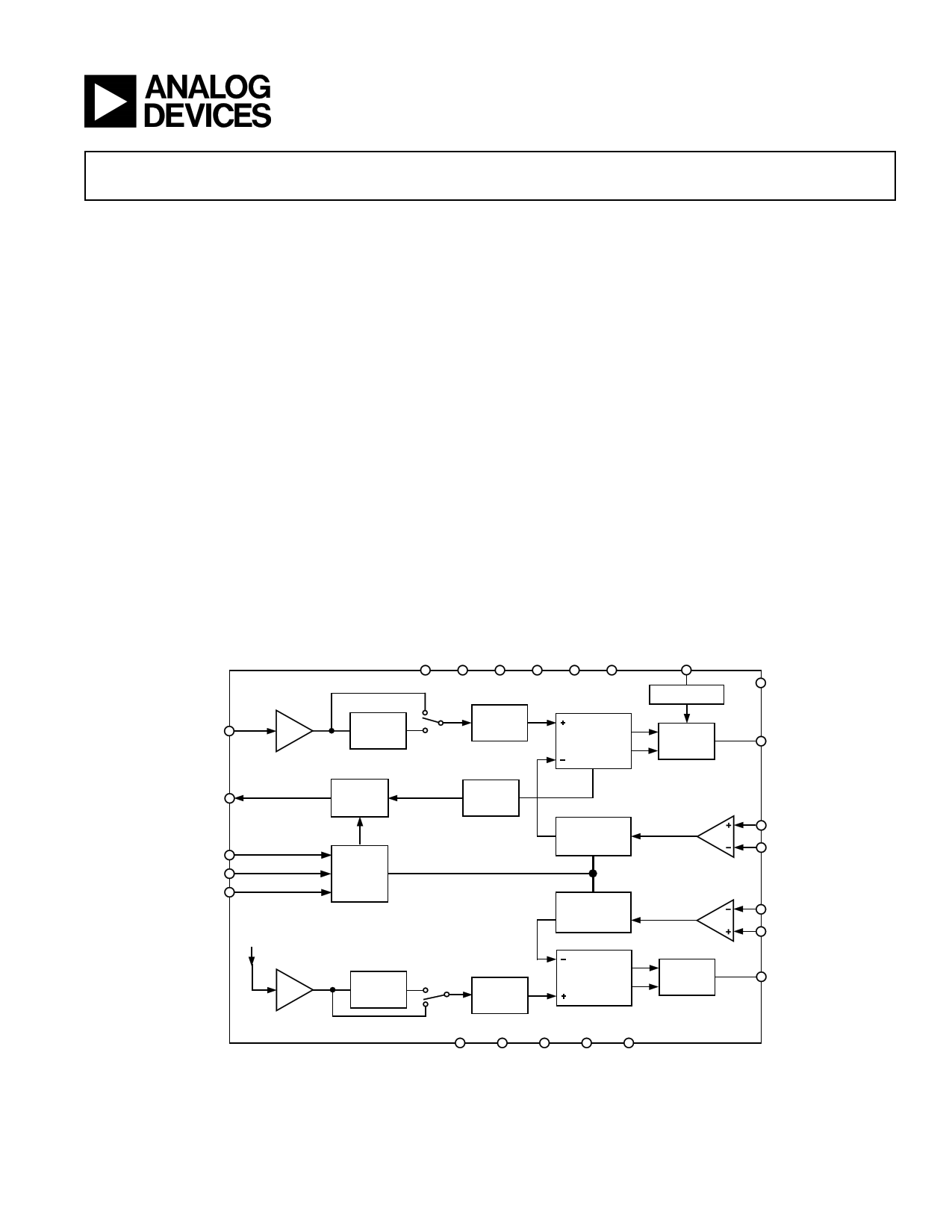
FUNCTIONAL BLOCK DIAGRAM
ADF4251
REFIN
VDD1 VDD2 VDD3 DVDD VP1
VP2
؋2
DOUBLER
4-BIT R
COUNTER
PHASE
FREQUENCY
DETECTOR
RSET
REFERENCE
CHARGE
PUMP
CE
CPRF
MUXOUT
CLK
DATA
LE
FROM
REFIN
OUTPUT
MUX
24-BIT
DATA
REGISTER
؋2
DOUBLER
LOCK
DETECT
FRACTIONAL N
RF DIVIDER
INTEGER N
IF DIVIDER
15-BIT R
COUNTER
PHASE
FREQUENCY
DETECTOR
CHARGE
PUMP
RFINA
RFINB
IFINB
IFINA
CPIF
AGND1 AGND2 DGND CPGND1 CPGND2
REV. 0
Information furnished by Analog Devices is believed to be accurate and
reliable. However, no responsibility is assumed by Analog Devices for its
use, nor for any infringements of patents or other rights of third parties that
may result from its use. No license is granted by implication or otherwise
under any patent or patent rights of Analog Devices. Trademarks and
registered trademarks are the property of their respective owners.
One Technology Way, P.O. Box 9106, Norwood, MA 02062-9106, U.S.A.
Tel: 781/329-4700
www.analog.com
Fax: 781/326-8703 © 2003 Analog Devices, Inc. All rights reserved.
1 page 
Mnemonic
CPRF
CPGND1
RFINA
RFINB
AGND1
MUXOUT
REFIN
CE
DGND
CLK
DATA
LE
RSET
AGND2
IFINB
IFINA
DVDD
CPGND2
CPIF
VP2
VDD2
VDD3
VDD1
VP1
ADF4251
PIN FUNCTION DESCRIPTIONS
Function
RF Charge Pump Output. This is normally connected to a loop filter that drives the input to an external VCO.
RF Charge Pump Ground
Input to the RF Prescaler. This small signal input is normally taken from the VCO.
Complementary Input to the RF Prescaler
Analog Ground for the RF Synthesizer
This multiplexer output allows either the RF or IF lock detect, the scaled RF or IF, or the scaled reference fre-
quency to be accessed externally.
Reference Input. This is a CMOS input with a nominal threshold of VDD/2 and an equivalent input resistance of
100 kW. This input can be driven from a TTL or CMOS crystal oscillator.
Chip Enable. A Logic Low on this bit powers down the device and puts the charge pump outputs into three-state.
A Logic High on this pin powers up the device, depending on the status of the software power-down bits.
Digital Ground for the Fractional Interpolator
Serial Clock Input. This serial clock is used to clock in the serial data to the registers. The data is latched into the
shift register on the CLK rising edge. This input is a high impedance CMOS input.
Serial Data Input. The serial data is loaded MSB first with the three LSBs being the control bits. This input is a
high impedance CMOS input.
Load Enable, CMOS Input. When LE goes high, the data stored in the shift registers is loaded into one of the
seven latches, the latch being selected using the control bits.
Connecting a resistor between this pin and ground sets the minimum charge pump output current. The relationship
between ICP and RSET is:
1.6875
ICP MIN = RSET
Therefore, with RSET = 2.7 kW, ICP MIN = 0.625 mA.
Ground for the IF Synthesizer
Complementary Input to the IF Prescaler
Input to the IF Prescaler. This small signal input is normally taken from the IF VCO.
Positive Power Supply for the Fractional Interpolator Section. Decoupling capacitors to the ground plane should
be placed as close as possible to this pin. DVDD must have the same voltage as VDD1, VDD2, and VDD3.
IF Charge Pump Ground
IF Charge Pump Output. This is normally connected to a loop filter that drives the input to an external VCO.
IF Charge Pump Power Supply. Decoupling capacitors to the ground plane should be placed as close as possible
to this pin. This voltage should be greater than or equal to VDD2.
Positive Power Supply for the IF Section. Decoupling capacitors to the ground plane should be placed as close as
possible to this pin. VDD2 has a value 3 V ± 10%. VDD2 must have the same voltage as VDD1, VDD3, and DVDD.
Positive Power Supply for the RF Digital Section. Decoupling capacitors to the ground plane should be placed as close
as possible to this pin. VDD3 has a value 3 V ± 10%. VDD3 must have the same voltage as VDD1, VDD2, and DVDD.
Positive Power Supply for the RF Analog Section. Decoupling capacitors to the ground plane should be placed as close
as possible to this pin. VDD1 has a value 3 V ± 10%. VDD1 must have the same voltage as VDD2, VDD3, and DVDD.
RF Charge Pump Power Supply. Decoupling capacitors to the ground plane should be placed as close as possible
to this pin. This voltage should be greater than or equal to VDD1.
REV. 0
–5–
5 Page 
CIRCUIT DESCRIPTION
Reference Input Section
The reference input stage is shown in Figure 3. SW1 and SW2
are normally closed switches. SW3 is normally open. When
power-down is initiated, SW3 is closed and SW1 and SW2 are
opened. This ensures that there is no loading of the REFIN pin
on power-down.
POWER-DOWN
CONTROL
ADF4251
REFIN = the reference input frequency, D = RF REFIN Doubler
Bit, R = the preset divide ratio of the binary 4-bit program-
mable reference counter (1 to 15), INT = the preset divide ratio of
the binary 8-bit counter (31 to 255), MOD = the preset modulus
ratio of binary 12-bit programmable FRAC counter (2 to 4095),
and FRAC = the preset fractional ratio of the binary 12-bit
programmable FRAC counter (0 to MOD).
RF N DIVIDER
N = INT + FRAC/MOD
NC 100k⍀
REFIN NC
SW2
SW1
SW3
NO
BUFFER
XOEB
TO R
COUNTER
REFOUT
NC = NORMALLY CLOSED
NO = NORMALLY OPEN
Figure 3. Reference Input Stage
RF and IF Input Stage
The RF input stage is shown in Figure 4. The IF input stage is
the same. It is followed by a two-stage limiting amplifier to
generate the CML clock levels needed for the N counter.
BIAS
GENERATOR
1.6V
2k⍀
2k⍀
VDD1
RFINA
RFINB
AGND
Figure 4. RF Input Stage
RF INT Divider
The RF INT CMOS counter allows a division ratio in the PLL
feedback counter. Division ratios from 31 to 255 are allowed.
INT, FRAC, MOD, and R Relationship
The INT, FRAC, and MOD values, in conjunction with the
RF R counter, make it possible to generate output frequencies
that are spaced by fractions of the RF phase frequency detector
(PFD). The equation for the RF VCO frequency (RFOUT) is
RFOUT
=
FPFD
¥
Ê
ËÁ
INT
+
FRAC ˆ
MOD ¯˜
(1)
where RFOUT is the output frequency of external voltage controlled
oscillator (VCO).
( )FPFD
= REFIN
¥
1+ D
R
(2)
FROM RF
INPUT STAGE
N-COUNTER
INT
REG
THIRD-ORDER
FRACTIONAL
INTERPOLATOR
MOD
REG
FRAC
VALUE
TO PFD
Figure 5. N Counter
RF R Counter
The 4-bit RF R counter allows the input reference frequency
(REFIN) to be divided down to produce the reference clock to
the RF PFD. Division ratios from 1 to 15 are allowed.
IF R Counter
The 15-bit IF R counter allows the input reference frequency
(REFIN) to be divided down to produce the reference clock to
the IF PFD. Division ratios from 1 to 32767 are allowed.
IF Prescaler (P/P + 1)
The dual modulus IF prescaler (P/P + 1), along with the IF A
and B counters, enables the large division ratio, N, to be realized
(N = PB + A). Operating at CML levels, it takes the clock from
the IF input stage and divides it down to a manageable frequency
for the CMOS IF A and CMOS IF B counters.
IF A and B Counters
The IF A CMOS and IF B CMOS counters combine with the
dual modulus IF prescaler to allow a wide ranging division ratio
in the PLL feedback counter. The counters are guaranteed to
work when the prescaler output is 150 MHz or less.
Pulse Swallow Function
The IF A and IF B counters, in conjunction with the dual modulus
IF prescaler, make it possible to generate output frequencies
that are spaced only by the reference frequency divided by R.
See the Device Programming after Initial Power-Up section for
examples. The equation for the IF VCO (IFOUT) frequency is
[( ) ]IFOUT = P ¥ B + A ¥ FPFD
(3)
where IFOUT = the output frequency of the external voltage controlled
oscillator (VCO), P = the preset modulus of the IF dual modulus
prescaler, B = the preset divide ratio of the binary 12-bit counter
(3 to 4095), and A = the preset divide ratio of the binary 6-bit
swallow counter (0 to 63). FPFD is obtained using Equation 2.
REV. 0
–11–
11 Page | ||
| Páginas | Total 28 Páginas | |
| PDF Descargar | [ Datasheet ADF4251.PDF ] | |
Hoja de datos destacado
| Número de pieza | Descripción | Fabricantes |
| ADF4251 | Dual Fractional-N/Integer-N Frequency Synthesizer | Analog Devices |
| ADF4252 | Dual Fractional-N/Integer-N Frequency Synthesizer | Analog Devices |
| Número de pieza | Descripción | Fabricantes |
| SLA6805M | High Voltage 3 phase Motor Driver IC. |
Sanken |
| SDC1742 | 12- and 14-Bit Hybrid Synchro / Resolver-to-Digital Converters. |
Analog Devices |
|
DataSheet.es es una pagina web que funciona como un repositorio de manuales o hoja de datos de muchos de los productos más populares, |
| DataSheet.es | 2020 | Privacy Policy | Contacto | Buscar |