|
|
|
PDF CH1817 Data sheet ( Hoja de datos )
| Número de pieza | CH1817 | |
| Descripción | Family of Low Profile DAA Modules | |
| Fabricantes | ETC | |
| Logotipo | ||
Hay una vista previa y un enlace de descarga de CH1817 (archivo pdf) en la parte inferior de esta página. Total 7 Páginas | ||
|
No Preview Available !
www.DataSheet4U.com
CH1817
Family of Low Profile DAA Modules
INTRODUCTION
The CH1817 is a Family of Low Profile Data Access
Arrangement (DAA) Modules. They are compatible
with all modem chip sets. These devices have been
tested to meet or exceed FCC Part 68 requirements
and are Canadian DOC approvable. They are also
recognized by Underwriters Laboratories to UL 1459
Specifications.
The CH1817 modules are ultra small (1.0” x 1.0”
x0.35”) affording an easy integration into space-
sensitive designs, including laptop and hand-held
computer based products. The CH1817 family of
products may be socketed or mounted directly onto a
Printed Circuit Board (PCB). The telephone line
connection is made through TIP and RING to an RJ-11
jack or equivalent.
The CH1817 is intended for use with FAX/modem chip
sets that have a data throughput of up through
V.32bis. For High Speed Applications, Cermetek
recommends the CH1837A.
FEATURES
• Low Profile, Ultra small size: 1.0” x 1.0” x 0.35”
• Complete DAA function
• Ring detection
• Built-in 2-wire to 4-wire conversion
• Lightweight
• Multimedia compatible
• +5V operation
• 1000 VAC isolation
• 800 Volt surge protection
• V.32bis/14,400bps, applications
• UL1459 recognized
• CH1817-L: Low power consumption and Common
mode noise rejection filter
• CH1817-LM (special order): Reduced transmit
attenuation
• CH1817-D: Differential transmission input and 0dB
transmission insertion loss.
DataShee
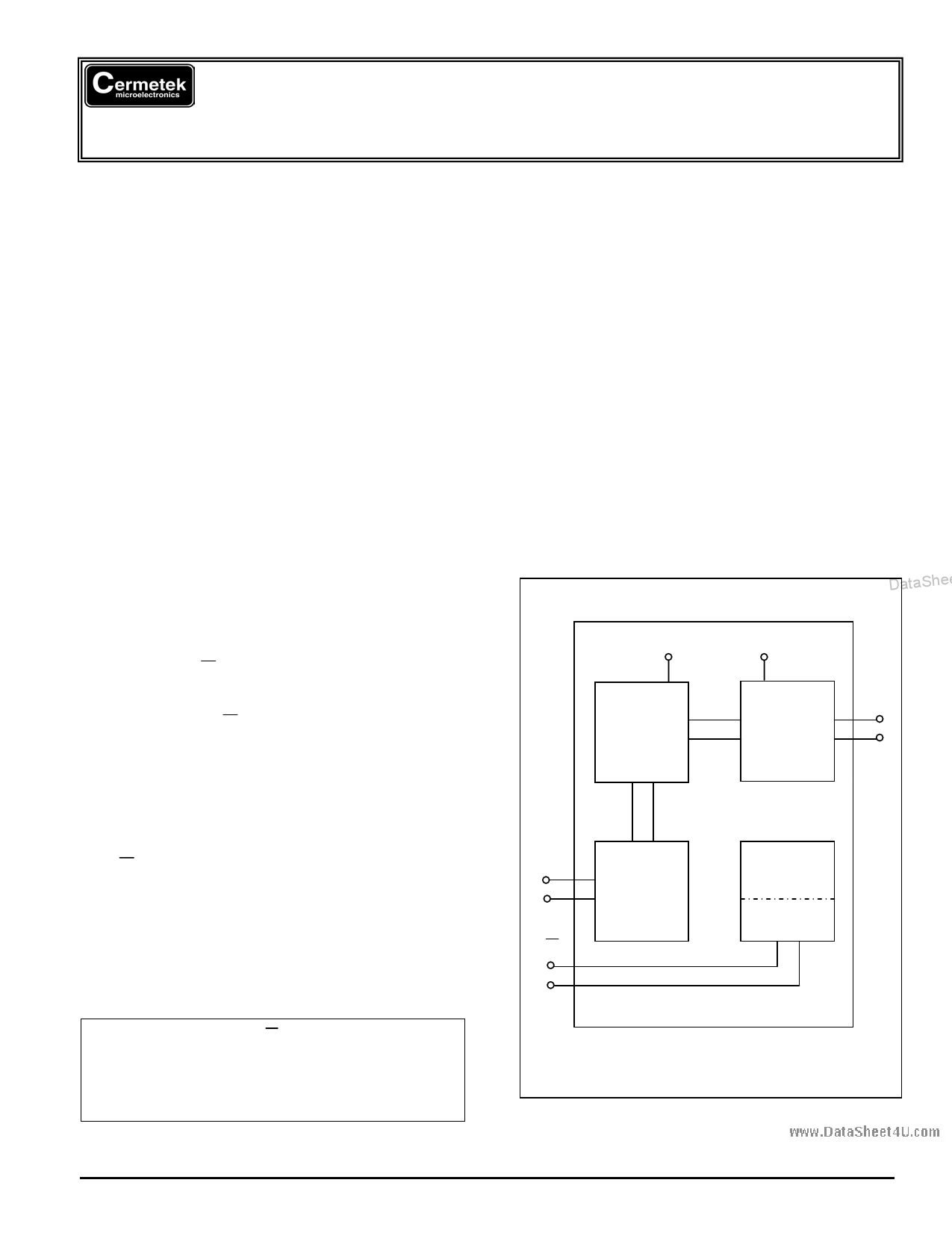
FUNCTIONAL DESCRIPTION
DataSheet4U.com
Ring Detection. Referring to the block diagram in
Figure 1, incoming ring detection is performed by the
CH1817 and the RI pin is set Low during the 2 second
(typical) ring period and is restored to High for the 4
seconds (typical) between rings. During incoming ring
signal activity, the RI output is pulsed at the same
frequency as the ringing signal, typically 20Hz. Figure
2 contains additional external circuitry which may be
used to provide an envelope indication of the ring
signal. The internal ring detection circuit is designed
to deter false indications due to pulse dialing or noise
on the line.
VCC
ISOLATION
GND
SURGE
AND
PROTECTION
CIRCUITRY
TIP
RING
The RI output of the CH1817 is diode protected.
Therefore, an external pull-up resistor (R>100Kohm)
to +5V may be utilized to activate the ring detection
circuit when the CH1817 is not connected to power.
This can be handy in designs where power
consumption is of concern. When circuited in this
manner, there is virtually no current draw until a ring
signal is present.
XMIT
RCV
RI
HYBRID
2W/4W
CONVERTER
OFFHK
OFF-HOOK
SWITCH
RING DET.
RI
Output: Active low
Opto coupler, 30KΩ pull-up
Square wave: 15-68Hz (Typ. 20Hz)
Sensitivity: 38Vrms across Tip & Ring
DataSheet4U.com
Figure 1. CH1817 DAA Functional Block Diagram.
2002 Cermetek Microelectronics, Inc.
DataSheet4 U .com
Page 1
Document No. 607-0007 Revision B (01/02)
1 page 
www.DataSheet4U.com
Cermetek Microelectronics, Inc.
CH1817 Family of Low Profile DAA Modules
Figure 3. Telephone Line Interface.
1. RJ-11 Jacks must be provided by one of the
vendors on the list. Refer to Application Note
#130, Summary of Recommended Suppliers.
et4U.com
2. Current Line Device: F1 and F2 – 1.25amp.
A. UL 1459 must use a current limit device. A
Poly Fuse is recommended as this device
resets automatically after each power surge.
B. Resistors (10ohm carbon film or SMD 1/8W
minimum) may be used for noDnataUSLheet4U.com
applications.
3. Over Voltage and Lightning Protection.
A. DOC (Canada) may require external current
limiting devices. Use 1ohm resistors (carbon
film or SMD parts 1/8W minimum) in each lead
(TIP and RING). You may substitute fuses or
the Poly Fuse described in Section 2.
B. For lightning prone areas where there are
more than 2 storms per year, provide an earth
ground connection and use a three terminal
sidactor or similar device that provides metallic
and longitudinal protection. This must also
include the current protection in Section 2.
Figure 4. Low Power Ring Detection.
4. EMI/RFI Suppression.
The capacitor/ inductor network should be located
as close to the RJ-11 Jack as possible with an
excellent ground path to the chassis. Capacitors
C1 and C2 should not exceed 0.005µF. They
must have a rating of 1.5KV and typically have a
value of 0.001µF ± 20%. Inductors L1 and L2 are
ferrite cylinders and provide attenuation to high
frequencies from system level components
external to the CH1817. The required values must
be empirically determined for each product design
DataSheet4U.com
DataShee
2002 Cermetek Microelectronics, Inc.
DataSheet4 U .com
Page 5
Document No. 607-0007 Revision B (01/02)
5 Page | ||
| Páginas | Total 7 Páginas | |
| PDF Descargar | [ Datasheet CH1817.PDF ] | |
Hoja de datos destacado
| Número de pieza | Descripción | Fabricantes |
| CH1817 | Family of Low Profile DAA Modules | ETC |
| Número de pieza | Descripción | Fabricantes |
| SLA6805M | High Voltage 3 phase Motor Driver IC. |
Sanken |
| SDC1742 | 12- and 14-Bit Hybrid Synchro / Resolver-to-Digital Converters. |
Analog Devices |
|
DataSheet.es es una pagina web que funciona como un repositorio de manuales o hoja de datos de muchos de los productos más populares, |
| DataSheet.es | 2020 | Privacy Policy | Contacto | Buscar |