|
|
PDF S29AL016M Data sheet ( Hoja de datos )
| Número de pieza | S29AL016M | |
| Descripción | 16 MEGABIT (2M X 8 BIT / I M X 16 BIT) 3.0 VOLT ONLY BOOT SECTOR FLASH MEMORY | |
| Fabricantes | SPANSION | |
| Logotipo |  |
|
Hay una vista previa y un enlace de descarga de S29AL016M (archivo pdf) en la parte inferior de esta página. Total 30 Páginas | ||
|
No Preview Available !
www.DataSheet4U.com
S29AL016M
16 Megabit (2 M x 8-Bit/1 M x 16-Bit)
3.0 Volt-only Boot Sector Flash Memory
featuring MirrorBitTM technology
Data Sheet
Distinctive Characteristics
DATASHEET
Architectural Advantages
Single power supply operation
— 3 V for read, erase, and program operations
Manufactured on 0.23 µm MirrorBitTM process
technology
— 400 nA standby mode current
— 15 mA read current
— 40 mA program/erase current
— 400 nA Automatic Sleep mode current
Package options
SecSiTM (Secured Silicon) Sector region
— 48-ball Fine-pitch BGA
— 128-word/256-byte sector for permanent, secure
identification through an 8-word/16-byte random
Electronic Serial Number, accessible through a
— 64-ball Fortified BGA
— 48-pin TSOP
command sequence
— May be programmed and locked at the factory or by
the customer
Flexible sector architecture
— One 16 Kbyte, two 8 Kbyte, one 32 Kbyte, and thirty-
one 64 Kbyte sectors (byte mode)
— One 8 Kword, two 4 Kword, one 16 Kword, and thirty-
one 32 Kword sectors (word mode)
Software Features
— Program Suspend & Resume: read other sectors
before programming operation is completed
— Erase Suspend & Resume: read/program other
sectors before an erase operation is completed
— Data# polling & toggle bits provide status
— Unlock Bypass Program command reduces overall
multiple-word programming time
Compatibility with JEDEC standards
— CFI (Common Flash Interface) compliant: allows host
—
Provides pinout and
power supply flash,
asnodftwsuapreercioormipnaatdibveilirttyenfotDrwsariinttaegSleh- eet4U.comsdyesvtiecems
to
identify
and
accommodate
multiple
flash
protection
Top or bottom boot block configurations available
100,000 erase cycle typical per sector
20-year typical data retention
Performance Characteristics
Hardware Features
— Sector Protection: hardware-level method of
preventing write operations within a sector
— Temporary Sector Unprotect: VID-level method of
changing code in locked sectors
— Hardware reset input (RESET#) resets device
High performance
— Ready/Busy# output (RY/BY#) indicates program or
— 90 ns access time
erase cycle completion
— 0.7 s typical sector erase time
Low power consumption (typical values at 5 MHz)
DataShee
DataSheet4U.com
DataSheet4 U .com
Publication Number S29AL016M_00 Revision A Amendment 4 Issue Date April 21, 2004
DataSheet4U.com
1 page 
www.DataSheet4U.com
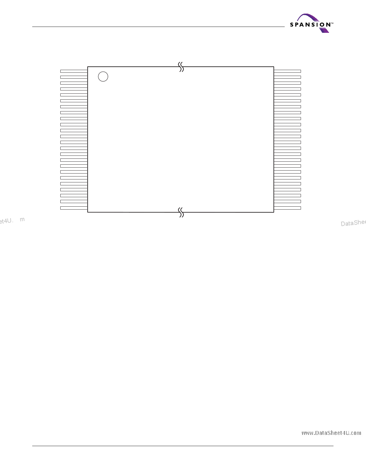
Connection Diagrams
et4U.com
A15
A14
A13
A12
A11
A10
A9
A8
A19
NC
WE#
RESET#
NC
NC
RY/BY#
A18
A17
A7
A6
A5
A4
A3
A2
A1
1
2
3
4
5
6
7
8
9
10
11
12
13
14
15
16
17
18
19
20
21
22
23
24
Standard TSOP
DataSheet4U.com
48 A16
47 BYTE#
46 VSS
45 DQ15/A-1
44 DQ7
43 DQ14
42 DQ6
41 DQ13
40 DQ5
39 DQ12
38 DQ4
37 VCC
36 DQ11
35 DQ3
34 DQ10
33 DQ2
32 DQ9
31 DQ1
30 DQ8
29 DQ0
28 OE#
27 VSS
26 CE#
25 A0
DataShee
DataSheet4U.com
April 21, 2004 S29AL016M_00A4
DataSheet4 U .com
S29AL016M
DataSheet4U.com
6
5 Page 
www.DataSheet4U.com
The internal state machine is set for reading array data upon device power-up,
or after a hardware reset. This ensures that no spurious alteration of the mem-
ory content occurs during the power transition. No command is necessary in
this mode to obtain array data. Standard microprocessor read cycles that as-
sert valid addresses on the device address inputs produce valid data on the
device data outputs. The device remains enabled for read access until the com-
mand register contents are altered.
See “Reading Array Data” for more information. Refer to the AC Read Operations
table for timing specifications and to Figure 13 for the timing diagram. ICC1 in the
DC Characteristics table represents the active current specification for reading
array data.
et4U.com
Writing Commands/Command Sequences
To write a command or command sequence (which includes programming data
to the device and erasing sectors of memory), the system must drive WE# and
CE# to VIL, and OE# to VIH.
For program operations, the BYTE# pin determines whether the device accepts
program data in bytes or words. Refer to “Word Configuration” for more
information.
The device features an Unlock Bypass mode to facilitate faster programming.
Once the device enters the Unlock Bypass mode, only two write cycles are re-
quired to program a word or byte, instead of four. The “Word Program Command
Sequence” section has details on programming data to the device using both
standard and Unlock Bypass command sequences.
An erase operation can erase oDnaetasSechteoer,t4mUu.cltoipmle sectors, or the entire device.
Tables 2 and 3 indicate the address space that each sector occupies. A “sector
address” consists of the address bits required to uniquely select a sector. The
“Command Definitions” section has details on erasing a sector or the entire chip,
or suspending/resuming the erase operation.
After the system writes the autoselect command sequence, the device enters the
autoselect mode. The system can then read autoselect codes from the internal
register (which is separate from the memory array) on DQ7–DQ0. Standard read
cycle timings apply in this mode. Refer to the “Autoselect Mode” and “Autoselect
Command Sequence” sections for more information.
ICC2 in the DC Characteristics table represents the active current specification for
the write mode. The “AC Characteristics” section contains timing specification ta-
bles and timing diagrams for write operations.
Program and Erase Operation Status
During an erase or program operation, the system may check the status of the
operation by reading the status bits on DQ7–DQ0. Standard read cycle timings
and ICC read specifications apply. Refer to “Write Operation Status” for more in-
formation, and to “AC Characteristics” for timing diagrams.
Standby Mode
When the system is not reading or writing to the device, it can place the device
in the standby mode. In this mode, current consumption is greatly reduced, and
the outputs are placed in the high impedance state, independent of the OE#
input.
DataSheet4U.com
April 21, 2004 S29AL016M_00A4
DataSheet4 U .com
S29AL016M
DataSheet4U.com
DataShee
12
11 Page | ||
| Páginas | Total 30 Páginas | |
| PDF Descargar | [ Datasheet S29AL016M.PDF ] | |
Hoja de datos destacado
| Número de pieza | Descripción | Fabricantes |
| S29AL016D | 16 MEGABIT CMOS 3.0 VOLT ONLY BOOT SECTOR FLASH MEMORY | SPANSION |
| S29AL016J | Boot Sector Flash | Cypress Semiconductor |
| S29AL016J | 16 Megabit (2 M x 8-Bit/1 M x 16-Bit) CMOS 3.0 Volt-only Boot Sector Flash Memory | Spansion |
| S29AL016M | 16 MEGABIT (2M X 8 BIT / I M X 16 BIT) 3.0 VOLT ONLY BOOT SECTOR FLASH MEMORY | SPANSION |
| Número de pieza | Descripción | Fabricantes |
| SLA6805M | High Voltage 3 phase Motor Driver IC. |
Sanken |
| SDC1742 | 12- and 14-Bit Hybrid Synchro / Resolver-to-Digital Converters. |
Analog Devices |
|
DataSheet.es es una pagina web que funciona como un repositorio de manuales o hoja de datos de muchos de los productos más populares, |
| DataSheet.es | 2020 | Privacy Policy | Contacto | Buscar |
