|
|
PDF ADD8707 Data sheet ( Hoja de datos )
| Número de pieza | ADD8707 | |
| Descripción | 12-Channel Gamma Buffers with VCOM and Regulator | |
| Fabricantes | Analog Devices | |
| Logotipo |  |
|
Hay una vista previa y un enlace de descarga de ADD8707 (archivo pdf) en la parte inferior de esta página. Total 20 Páginas | ||
|
No Preview Available !
FEATURES
12 precision gamma reference outputs
Mask-programmable gamma resistors:
0.2% resolution and 0.1% accuracy
Mask programmable voltage regulator: 0.4% accuracy
Upper 6 buffers swing to VDD
Lower 6 buffers swing to GND
Single-supply operation: 7.5 V to 16 V
Gamma current drive: 15 mA per channel
VCOM peak output current: 250 mA
Outputs stable under load conditions
48-lead, Pb-free LFCSP package
APPLICATIONS
LCD TV panels
LCD monitor panels
PRODUCT OVERVIEW
The ADD8707 is a 12-channel integrated gamma reference with
VCOM for use in LCD TV and monitor panels. The output
buffers feature high current drive and low offset voltage to
provide an accurate and stable gamma curve. The top six
channels swing to VDD and the lower six channels swing to
GND.
Integrating the gamma setup resistors drastically reduces the
external component count while increasing the gamma curve
accuracy. To accommodate multiple column drivers and panel
architectures, the ADD8707 is mask-programmable to a 0.2%
resolution using the on-chip 500 resistor string. An on-board
voltage regulator provides a fixed input for the resistor string,
isolating the gamma curve from supply ripple.
The ADD8707 is specified over the temperature range of
–40°C to +105°C and comes in a 48-lead, Pb-free, lead frame
chip-scale package.
12-Channel Gamma Buffers
with VCOM and Regulator
ADD8707
FUNCTIONAL BLOCK DIAGRAM
MASK-PROGRAMMABLE
REGULATOR RESISTORS
FB
700Ω*
GND
+
1.2V –
VIN11
VIN10
VIN8
VIN7
VIN6
VIN5
700Ω*
700Ω*
MASK-
PROGRAMMABLE
GAMMA RESISTORS
700Ω*
700Ω*
700Ω*
700Ω*
VIN3
VIN2
VIN1
700Ω*
700Ω*
700Ω*
VCOM
GAMMA
BUFFERS
VCOM OUT
VOUT12
VOUT11
VOUT10
VOUT9
VOUT8
VOUT7
VOUT6
VOUT5
VOUT4
VOUT3
VOUT2
VOUT1
*ESD PROTECTION RESISTORS
Figure 1. 48-Lead LFCSP
Rev. A
Information furnished by Analog Devices is believed to be accurate and reliable.
However, no responsibility is assumed by Analog Devices for its use, nor for any
infringements of patents or other rights of third parties that may result from its use.
Specifications subject to change without notice. No license is granted by implication
or otherwise under any patent or patent rights of Analog Devices. Trademarks and
registered trademarks are the property of their respective owners.
One Technology Way, P.O. Box 9106, Norwood, MA 02062-9106, U.S.A.
Tel: 781.329.4700
www.analog.com
Fax: 781.326.8703 © 2004 Analog Devices, Inc. All rights reserved.
1 page 
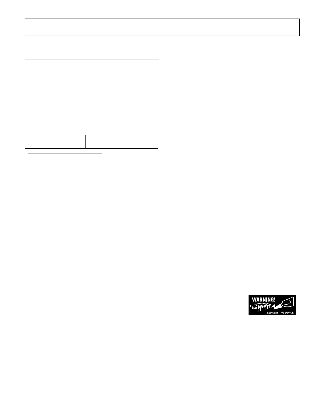
ABSOLUTE MAXIMUM RATINGS
Table 2.
Parameter
Supply Voltage (VDD)
Input Voltage
Storage Temperature Range
Operating Temperature Range1
Lead Temperature Range (Soldering 10 sec)
Junction Temperature
ESD Tolerance (HBM)
ESD Tolerance (MM)
Rating
18 V
−0.5 V to VDD
−65°C to +150°C
−40°C to +105°C
300°C
150°C
±3000 V
±100 V
Table 3. Thermal Resistance
Package Type
θJA2 θJA3 Unit
48-Lead LFCSP (CP)
28.3 47.7 °C/W
1 See the Applications Information section.
2 θJA for exposed pad soldered to JEDEC 4-layer board.
3 θJA for exposed pad not soldered down.
ADD8707
Stresses above those listed under Absolute Maximum Ratings
may cause permanent damage to the device. This is a stress
rating only; functional operation of the device at these or any
other conditions above those indicated in the operational
section of this specification is not implied. Exposure to absolute
maximum rating conditions for extended periods may affect
device reliability.
ESD CAUTION
ESD (electrostatic discharge) sensitive device. Electrostatic charges as high as 4000 V readily accumulate on
the human body and test equipment and can discharge without detection. Although this product features
proprietary ESD protection circuitry, permanent damage may occur on devices subjected to high energy
electrostatic discharges. Therefore, proper ESD precautions are recommended to avoid performance
degradation or loss of functionality.
Rev. A | Page 5 of 20
5 Page 
11
10V PULSE
10 120pF
9 320pF
520pF
8 1nF
10nF
7
6
5
4
3
2
1
0
–200 0 200 400 600 800 1000 1200 1400 1600 1800
TIME (ns)
Figure 21. Gamma Buffers Transient Load Response vs. Capacitive Loading
ADD8707
8.8
8.7
8.6
8.5
8.4
8.3
8.2
8.1
–20
0 20 40 60 80 100
TEMPERATURE (°C)
Figure 22. Supply Current vs. Temperature
120
Rev. A | Page 11 of 20
11 Page | ||
| Páginas | Total 20 Páginas | |
| PDF Descargar | [ Datasheet ADD8707.PDF ] | |
Hoja de datos destacado
| Número de pieza | Descripción | Fabricantes |
| ADD8701 | 12-Channel Gamma Buffers with VCOM Buffer | Analog Devices |
| ADD8701 | 12-Channel Gamma Buffers with VCOM Buffer | Analog Devices |
| ADD8702 | 12-Channel Gamma Buffers | Analog Devices |
| ADD8704 | 16 V Quad Operational Amplifier | Analog Devices |
| Número de pieza | Descripción | Fabricantes |
| SLA6805M | High Voltage 3 phase Motor Driver IC. |
Sanken |
| SDC1742 | 12- and 14-Bit Hybrid Synchro / Resolver-to-Digital Converters. |
Analog Devices |
|
DataSheet.es es una pagina web que funciona como un repositorio de manuales o hoja de datos de muchos de los productos más populares, |
| DataSheet.es | 2020 | Privacy Policy | Contacto | Buscar |
