|
|
|
PDF HPC167064 Data sheet ( Hoja de datos )
| Número de pieza | HPC167064 | |
| Descripción | (HPC467064 / HPC167064) High-Performance microController with a 16k UV Erasable CMOS EPROM | |
| Fabricantes | National Semiconductor | |
| Logotipo | ||
Hay una vista previa y un enlace de descarga de HPC167064 (archivo pdf) en la parte inferior de esta página. Total 30 Páginas | ||
|
No Preview Available !
PRELIMINARY
August 1992
HPC167064 HPC467064 High-Performance
microController with a 16k UV Erasable CMOS EPROM
General Description
The HPC167064 is a member of the HPC family of High
Performance microControllers Each member of the family
has the same core CPU with a unique memory and I O
configuration to suit specific applications The HPC167064
has a 16 kbyte high-speed UV-erasable electrically pro-
grammable CMOS EPROM This is ideally suited for appli-
cations where fast turnaround pattern experimentation and
code confidentiality are important requirements The
HPC167064 can serve as a stand-alone emulator for either
the HPC16064 or the HPC16083 Two configuration regis-
ters have been added for emulation of the different chips
The on-chip EPROM replaces the presently available user
ROM space The on-chip EPROM can be programmed via a
DATA I O UNISITE There are security features added to
the chip to implement READ ENCRYPTED READ and
WRITE privileges for the on-chip EPROM These defined
privileges are intended to deter theft alteration or uninten-
tional destruction of user code Each part is fabricated in
National’s advanced microCMOS technology This process
combined with an advanced architecture provides fast flex-
ible I O control efficient data manipulation and high speed
computation
The HPC devices are complete microcomputers on a single
chip All system timing internal logic EPROM RAM and
I O are provided on the chip to produce a cost effective
solution for high performance applications On-chip func-
tions such as UART up to eight 16-bit timers with 4 input
capture registers vectored interrupts WATCHDOGTM logic
and MICROWIRE PLUSTM provide a high level of system
integration The ability to address up to 64k bytes of exter-
nal memory enables the HPC to be used in powerful appli-
cations typically performed by microprocessors and expen-
sive peripheral chips
The microCMOS process results in very low current drain
and enables the user to select the optimum speed power
product for his system The IDLE and HALT modes provide
further current savings The HPC167064 is available only in
68-pin LDCC package
Features
Y HPC family core features
16-bit architecture both byte and word operations
16-bit data bus ALU and registers
64 kbytes of direct memory addressing
FAST 200 ns for fastest instruction when using
20 0 MHz clock 134 ns at 30 0 MHz
High code efficiency most instructions are single
byte
16 x 16 multiply and 32 x 16 divide
Eight vectored interrupt sources
Four 16-bit timer counters with 4 synchronous out-
puts and WATCHDOG logic
MICROWIRE PLUS serial I O interface
CMOS very low power with two power save modes
IDLE and HALT
Y 16 kbytes high speed UV erasable electrically program-
mable CMOS EPROM
Y Stand-alone emulation of HPC16083 and HPC16064
family
Y EPROM and configuration bytes programmable by
DATA I O UNISITE with Pinsite Module
Y Four selectable levels of security to protect on-chip
EPROM contents
Y UART full duplex programmable baud rate
Y Four additional 16-bit timer counters with pulse width
modulated outputs
Y Four input capture registers
Y 52 general purpose I O lines (memory mapped)
Y Commercial (0 C to a70 C) and military (b55 C to
a125 C) temperature ranges for 20 0 MHz commercial
(0 C to a70 C) for 30 0 MHz
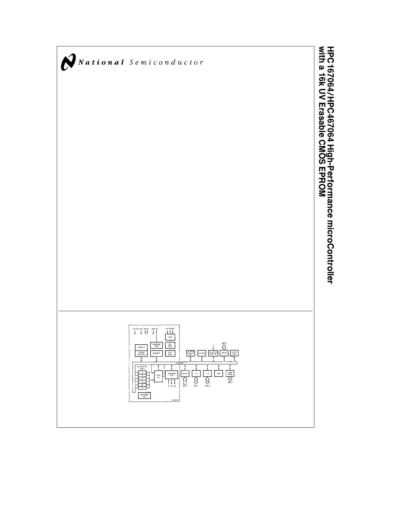
Block Diagram (HPC167064 with 16k EPROM shown)
Series 32000 and TRI-STATE are registered trademarks of National Semiconductor Corporation
MICROWIRE PLUSTM and WATCHDOGTM are trademarks of National Semiconductor Corporation
UNIX is a registered trademark of AT T Bell Laboratories
IBM and PC-AT are registered trademarks of International Business Machines Corp
SunOSTM is a trademark of Sun Microsystems
C1995 National Semiconductor Corporation TL DD11046
TL DD 11046 – 1
RRD-B30M105 Printed in U S A
1 page 
30 MHz
AC Electrical Characteristics
(See Notes 1 and 4 and Figures 1 thru 5 ) VCC e 5V g10% TA e 0 C to a70 C for HPC467064
Symbol and Formula
fC
tC1 e 1 fC
tCKIH
tCKIL
tC e 2 fC
tWAIT e tC
tDC1C2R
tDC1C2F
fU e fC 8
fMW
fXIN e fC 22
tXIN e tC
Parameter
Min Max
CKI Operating Frequency
CKI Clock Period
CKI High Time
CKI Low Time
CPU Timing Cycle
CPU Wait State Period
Delay of CK2 Rising Edge after CKI Falling Edge
Delay of CK2 Falling Edge after CKI Falling Edge
2 30
33 500
22 5
22 5
66
66
0 55
0 55
External UART Clock Input Frequency
External MICROWIRE PLUS Clock Input Frequency
3 75
1 875
External Timer Input Frequency
Pulse Width for Timer Inputs
1 364
66
Units
MHz
ns
ns
ns
ns
ns
ns
ns
MHz
MHz
MHz
ns
Notes
(Note 2)
(Note 2)
tUWS
tUWH
tUWV
tSALE e tC a 40
tHWP e tC a 10
tHAE e tC a 85
tHAD e tC a 85
tBF e tC a 66
tBE e tC a 66
tUAS
tUAH
tRPW
tOE
tOD
tDRDY
tWDW
tUDS
tUDH
tA
tDC1ALER
tDC1ALEF
tDC2ALER e tC a 20
tDC2ALEF e tC a 20
tLL e tC b 9
tST e tC b 7
tVP e tC b 5
MICROWIRE Setup Time Master
MICROWIRE Setup Time Slave
MICROWIRE Hold Time Master
MICROWIRE Hold Time Slave
MICROWIRE Output Valid Time Master
MICROWIRE Output Valid Time Slave
HLD Falling Edge before ALE Rising Edge
HLD Pulse Width
HLDA Falling Edge after HLD Falling Edge
HLDA Rising Edge after HLD Rising Edge
Bus Float after HLDA Falling Edge
Bus Enable after HLDA Rising Edge
Address Setup Time to Falling Edge of URD
Address Hold Time from Rising Edge of URD
URD Pulse Width
URD Falling Edge to Output Data Valid
Rising Edge of URD to Output Data Invalid
RDRDY Delay from Rising Edge of URD
UWR Pulse Width
Input Data Valid before Rising Edge of UWR
Input Data Hold after Rising Edge of UWR
WRRDY Delay from Rising Edge of UWR
Delay from CKI Rising Edge to ALE Rising Edge
Delay from CKI Rising Edge to ALE Falling Edge
Delay from CK2 Rising Edge to ALE Rising Edge
Delay from CK2 Falling Edge to ALE Falling Edge
ALE Pulse Width
Setup of Address Valid before ALE Falling Edge
Hold of Address Valid after ALE Falling Edge
100
20
20
50
50
150
90
76
151
135
99
99
10
10
100
0 60
5 45
70
40
10
20
70
0 35
0 35
37
37
24
9
11
ns
ns
ns
ns
ns
ns (Note 3)
ns
ns (Note 5)
ns (Note 5)
ns
ns
ns
ns
ns (Note 6)
ns
ns
ns
ns
ns
ns (Notes 1 2)
ns (Notes 1 2)
ns
ns
ns
ns
ns
5
5 Page 
Functional Modes of Operation (Continued)
Security Level 2
This security level prevents programming of the on-chip
EPROM or the ECON registers thereby providing WRITE
protection Read accesses to the on-chip EPROM or ECON
registers may be accomplished without constraint in
EPROM Read accesses to the on-chip EPROM may be
accomplished without constraint in NORMAL RUNNING
mode
Security Level 1
This security level prevents programming of the on-chip
EPROM or ECON registers thereby providing registers
write protection Read accesses to the on-chip ECON-regis-
ters may be accomplished without constraint in EPROM
mode Read accesses to the on-chip EPROM will produce
ENCRYPTED data in EPROM READ accesses to the on-
chip EPROM during NORMAL RUNNING mode are sub-
ject to Runtime Memory Protection Under Runtime Mem-
ory Protection only instruction opcodes stored within the
on-chip EPROM are allowed to access the EPROM as oper-
and If any other instruction opcode attempts to use the
contents of EPROM as an operand it will receive the hex
value ‘‘FF’’ The Runtime Memory Protection feature is de-
signed to prevent hostile software running from external
memory or on-chip RAM from reading secured EPROM
data Transfers of control into or out of the on-chip EPROM
(such as jump or branch) are not affected by Runtime Mem-
ory Protection Interrupt vector fetches from EPROM pro-
ceed normally and are not affected by Runtime Memory
Protection
Security Level 0
This security level prevents programming of the on-chip
EPROM or ECON registers thereby providing write protec-
tion Read accesses to the on-chip ECON registers may be
accomplished without constraint in EPROM mode READ
accesses to the on-chip EPROM are NOT ALLOWED in
EPROM mode Such accesses will return data value ‘‘FF’’
hex Runtime Memory Protection is enforced as in security
level 1
These four levels of security help ensure that the user
EPROM code is not tampered with in a test fixture and that
code executing from RAM or external memory does not
dump the user algorithm
An erasure system should be calibrated periodically The
distance from lamp to unit should be maintained at one inch
The erasure time increases as the square of the distance (If
distance is doubled the erasure time increases by a factor of
4 ) Lamps lose intensity as they age When a lamp is
changed the distance has changed or the lamp has aged
the system should be checked to make certain full erasure
is occurring
Incomplete erasure will cause symptoms that can be mis-
leading Programmers components and even system de-
signs have been erroneously suspected when incomplete
erasure was the problem
Minimum HPC167064 Erasure Time
Light Intensity
(Micro-Watts cm2)
15 000
10 000
Erasure Time
(Minutes)
36
50
Memory Map of the HPC167064
The HPC167064 has 256 bytes of on-chip user RAM and
chip registers located at address 0000 – 01FF that is always
enabled and 256 bytes of on-chip RAM located at 0200 –
02FF that can be enabled or disabled It has 8 kbytes of on-
chip EPROM located at address 0E000 – 0FFFF that is al-
ways enabled and 8 kbytes of EPROM located at address
0C000 – 0DFFF that can be enabled or disabled
The ECON6 contains two bits ROM0 and RAM0 When
these bits are ‘‘1’’ (erased default) full 16 kbytes of ROM
and 512 bytes of RAM are enabled Programming a ‘‘0’’ to
these bits disables the lower 8k for the EPROM and upper
256 bytes for the RAM The ECON registers are only acces-
sible to the user during EPROM mode
Address In
EPROM Mode
7FFF
Address In Other
HPC Modes
Operation
Erasure Characteristics
The erasure characteristics of the HPC167064 are such that
erasure begins to occur when exposed to light with wave-
lengths shorter than approximately 4000 Angstroms ( ) It
should be noted that sunlight and certain types of fluores-
cent lamps have wavelengths in the 3000 –4000 range
After programming opaque labels should be placed over
the HPC167064’s window to prevent unintentional erasure
Covering the window will also prevent temporary functional
failure due to the generation of photo currents
The recommended erasure procedure for the HPC167064 is
exposure to short wave ultraviolet light which has a wave-
length of 2537 Angstroms ( ) The integrated dose (i e UV
intensity c exposure time) for erasure should be a minimum
of 30W-sec cm2
The HPC167064 should be placed within 1 inch of the lamp
tubes during erasure Some lamps have a filter on their
tubes which should be removed before erasure The era-
sure time table shows the minimum HPC167064 erasure
time for various light intensities
4000
3FFF
2000
1FFF
0000
FFFF
E000
DFFF
–C000
Enabled or
Disabled by
config logic
11
11 Page | ||
| Páginas | Total 30 Páginas | |
| PDF Descargar | [ Datasheet HPC167064.PDF ] | |
Hoja de datos destacado
| Número de pieza | Descripción | Fabricantes |
| HPC167064 | (HPC467064 / HPC167064) High-Performance microController with a 16k UV Erasable CMOS EPROM | National Semiconductor |
| Número de pieza | Descripción | Fabricantes |
| SLA6805M | High Voltage 3 phase Motor Driver IC. |
Sanken |
| SDC1742 | 12- and 14-Bit Hybrid Synchro / Resolver-to-Digital Converters. |
Analog Devices |
|
DataSheet.es es una pagina web que funciona como un repositorio de manuales o hoja de datos de muchos de los productos más populares, |
| DataSheet.es | 2020 | Privacy Policy | Contacto | Buscar |