|
|
|
PDF MK2049-01 Data sheet ( Hoja de datos )
| Número de pieza | MK2049-01 | |
| Descripción | Communications Clock PLL | |
| Fabricantes | Integrated Circuit Systems | |
| Logotipo | ||
Hay una vista previa y un enlace de descarga de MK2049-01 (archivo pdf) en la parte inferior de esta página. Total 11 Páginas | ||
|
No Preview Available !
MK2049-01
Communications Clock PLL
Description
The MK2049 is a Phase-Locked Loop (PLL) based
clock synthesizer, which accepts an 8 kHz clock
input as a reference and generates T1, E1, T3, E3,
and OC3 frequencies. The device can also accept a
T1, E1, T3, or E3 input clock and provide the
same output for loop timing. All outputs are
frequency locked together and to the input. This
allows for the generation of locked clocks to an
8 kHz backplane clock, simplifying clock
distribution in communications systems.
MicroClock can customize this device for many
other different frequencies. Contact your
MicroClock representative for more details.
For a fixed input-output phase relationship, refer
to the MK2049-02, -03, or -3x. The MK2049-3x
are 3.3 V devices.
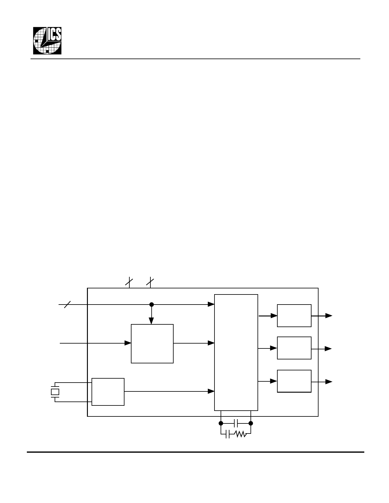
Block Diagram
VDD GND
44
Features
• Packaged in 20 pin SOIC
• Meets the TR62411, ETS300 011, and GR-1244
specification for MTIE, Pull-in/Hold-in Range,
Phase Transients, and Jitter Generation for
Stratum 3, 4, and 4E
• Accepts multiple inputs: 8 kHz backplane clock or
Loop Timing frequencies
• Locks to 8 kHz ±100 ppm (External mode)
• Exact internal ratios eliminate the need for external
dividers
• Zero ppm synthesis error in all output clocks.
• Output clock rates include T1, E1, T3, E3, and
OC3÷8
• 5 V ±5% operation
• Offered in Commercial and Industrial temperature
versions
FS3:0 4
Clock
Input
Reference
Crystal
X1
Crystal
Oscillator
X2
External/
Loop
Timing
Mux
PLL
Clock
Synthesis,
Control, and
Jitter
Attenuation
Circuitry
Output
Buffer
Output
Buffer
Output
Buffer
CLK1
CLK2
8 kHz
CAP1
CAP2
MDS 2049-01 J
1
Revision 040601
Integrated Circuit Systems, Inc. • 525 Race Street • San Jose • CA • 95126 • (408)295-9800tel •www.icst.com
1 page 
MK2049-01
Communications Clock PLL
LAYOUT AND EXTERNAL COMPONENTS
The MK2049-01 requires a minimum number of external components for proper operation. Decoupling
capacitors of 0.01µF must be connected between VDD and GND pins close to the chip (especially pins 4
and 7, 15 and 17), and 33 Ω series terminating resistors should be used on clock outputs with traces longer
than 1 inch (assuming 50 Ω traces). The loop filter components should be connected as close to the chip as
possible. Refer to the next section for more information.
PC Board Layout
A proper board layout is critical to the successful use of the MK2049. In particular, the CAP1 and CAP2 pins
are very sensitive to noise and leakage (CAP2 at pin 18 is the most sensitive). Traces must be as short as
possible and the two capacitors and resistor must be mounted next to the device as shown below. The
capacitor shown between pins 15 and 17, and the one between pins 5 and 7 are the power supply decoupling
capacitors. The high frequency output clocks on pins 8 and 9 should have a series termination of 33 Ω
connected close to the pin. Additional improvements will come from keeping all components on the same
side of the board, minimizing vias through other signal layers, and routing other signals away from the
MK2049. You may also refer to MAN05 for additional suggestions on layout of the crystal section.
The crystal traces should include pads for small capacitors from X1 and X2 to ground; these are used to
adjust the stray capacitance of the board to match the crystal load capacitance. The typical telecom reference
frequency is accurate to much less than 1 ppm, so the MK2049 may lock and run properly even if the board
capacitance is not adjusted with these fixed capacitors. However, ICS MicroClock recommends that the
adjustment capacitors be included to minimize the effects of variation in individual crystals, temperature,
and aging. The value of these capacitors (typically 0-4 pF) is determined once for a given board layout,
using the procedure described later in this section, titled “Determining the Crystal Frequency Adjustment
Capacitors”.
Optional;
see text
Cutout in ground and power plane.
cap Route all traces away from this area.
G
cap
1
2
3
V4
5
cap 6
7
resist.
8
resist.
9
10
20
19
18 resist.
17 G cap
16 cap
15 V
14
13
cap
V =connect to VDD
12 G =connect to GND
11
Figure 1. MK2049-01 Layout Example
MDS 2049-01 J
5
Revision 040601
Integrated Circuit Systems, Inc. • 525 Race Street • San Jose • CA • 95126 • (408)295-9800tel •www.icst.com
5 Page 
MK2049-01
Communications Clock PLL
Package Outline and Package Dimensions
(For current dimensional specifications, see JEDEC Publication No. 95.)
INDEX
AREA
12
D
EH
h x 45°
20 pin SOIC
Symbol
A
A1
B
C
D
E
e
H
h
L
Inches
Min Max
-- 0.104
0.0040 --
0.013 0.020
0.007 0.013
0.496 0.512
0.291 0.299
.050 BSC
0.394 0.419
0.01 0.029
0.016 0.050
Millimeters
Min Max
-- 2.65
0.10 --
0.33 0.51
0.18 0.33
12.60 13.00
7.40 7.60
1.27 BSC
10.01 10.64
0.25 0.74
0.41 1.27
A1
e
C
B
A
L
Ordering Information
Part/Order Number
MK2049-01S
MK2049-01STR
MK2049-01SI
MK2049-01SITR
Marking
MK2049-01S
MK2049-01S
MK2049-01SI
MK2049-01SI
Package
20 pin SOIC
Add Tape & Reel
20 pin SOIC
Add Tape & Reel
Temperature
0 to 70 °C
0 to 70 °C
-40 to 85 °C
-40 to 85 °C
While the information presented herein has been checked for both accuracy and reliability, ICS/MicroClock assumes no responsibility for either its use or for the infringement of
any patents or other rights of third parties, which would result from its use. No other circuits, patents, or licenses are implied. This product is intended for use in normal
commercial applications. Any other applications such as those requiring extended temperature range, high reliability, or other extraordinary environmental requirements are not
recommended without additional processing by ICS/MicroClock. ICS/MicroClock reserves the right to change any circuitry or specifications without notice. ICS/MicroClock
does not authorize or warrant any ICS/MicroClock product for use in life support devices or critical medical instruments.
MDS 2049-01 J
11
Revision 040601
Integrated Circuit Systems, Inc. • 525 Race Street • San Jose • CA • 95126 • (408)295-9800tel •www.icst.com
11 Page | ||
| Páginas | Total 11 Páginas | |
| PDF Descargar | [ Datasheet MK2049-01.PDF ] | |
Hoja de datos destacado
| Número de pieza | Descripción | Fabricantes |
| MK2049-01 | Communications Clock PLL | Integrated Circuit Systems |
| MK2049-02 | Communications Clock PLLs | Integrated Circuit Systems |
| MK2049-03 | Communications Clock PLLs | Integrated Circuit Systems |
| Número de pieza | Descripción | Fabricantes |
| SLA6805M | High Voltage 3 phase Motor Driver IC. |
Sanken |
| SDC1742 | 12- and 14-Bit Hybrid Synchro / Resolver-to-Digital Converters. |
Analog Devices |
|
DataSheet.es es una pagina web que funciona como un repositorio de manuales o hoja de datos de muchos de los productos más populares, |
| DataSheet.es | 2020 | Privacy Policy | Contacto | Buscar |