|
|
|
PDF MAX5812 Data sheet ( Hoja de datos )
| Número de pieza | MAX5812 | |
| Descripción | 12-Bit Low-Power / 2-Wire / Serial Voltage-Output DAC | |
| Fabricantes | Maxim Integrated | |
| Logotipo | ||
Hay una vista previa y un enlace de descarga de MAX5812 (archivo pdf) en la parte inferior de esta página. Total 13 Páginas | ||
|
No Preview Available !
19-2340; Rev 0; 1/02
12-Bit Low-Power, 2-Wire, Serial
Voltage-Output DAC
General Description
The MAX5812 is a single, 12-bit voltage-output, digital-to-
analog converter (DAC) with an I2C™-compatible 2-wire
interface that operates at clock rates up to 400kHz. The
device operates from a single 2.7V to 5.5V supply and
draws only 100µA at VDD = 3.6V. A low-power power-
down mode decreases current consumption to less than
1µA. The MAX5812 features three software-selectable
power-down output impedances: 100kΩ, 1kΩ, and high
impedance. Other features include an internal precision
Rail-to-Rail® output buffer and a power-on reset circuit
that powers up the DAC in the 100kΩ power-down mode.
The MAX5812 features a double-buffered I2C-compatible
serial interface that allows multiple devices to share a sin-
gle bus. All logic inputs are CMOS-logic compatible and
buffered with Schmitt triggers, allowing direct interfacing
to optocoupled and transformer-isolated interfaces. The
MAX5812 minimizes digital noise feedthrough by discon-
necting the clock (SCL) signal from the rest of the device
when an address mismatch is detected.
The MAX5812 is specified over the extended temperature
range of -40°C to +85°C and is available in a space-sav-
ing 6-pin SOT23 package. Refer to the MAX5811 for the
10-bit version.
Applications
Digital Gain and Offset Adjustments
Programmable Voltage and Current Sources
Programmable Attenuation
VCO/Varactor Diode Control
Low-Cost Instrumentation
Battery-Operated Equipment
Typical Operating Circuit
VDD
µC
SDA SCL
VDD
RP RP
RS
SCL
VDD
RS SDA MAX5812 OUT
RS
SCL VDD
RS
SDA MAX5812 OUT
Features
o Ultra-Low Supply Current
100µA at VDD = 3.6V
130µA at VDD = 5.5V
o 300nA Low-Power Power-Down Mode
o Single 2.7V to 5.5V Supply Voltage
o Fast 400kHz I2C-Compatible 2-Wire Serial
Interface
o Schmitt-Trigger Inputs for Direct Interfacing to
Optocouplers
o Rail-to-Rail Output Buffer Amplifier
o Three Software-Selectable Power-Down Output
Impedances
100kΩ, 1kΩ, and High Impedance
o Read-Back Mode for Bus and Data Checking
o Power-On Reset to Zero
o Miniature 6-Pin SOT23 Package
Ordering Information
PART
TEMP RANGE
PIN-
PACKAGE
TOP
MARK
MAX5812LEUT -40°C to +85°C 6 SOT23
AAYT
MAX5812MEUT -40°C to +85°C 6 SOT23
AAYV
MAX5812NEUT -40°C to +85°C 6 SOT23
AAYX
MAX5812PEUT -40°C to +85°C 6 SOT23
AAYZ
Selector Guide appears at end of data sheet.
Functional Diagram appears at end of data sheet.
Rail-to-Rail is a registered trademark of Nippon Motorola, Ltd.
I2C is a trademark of Philips Corporation.
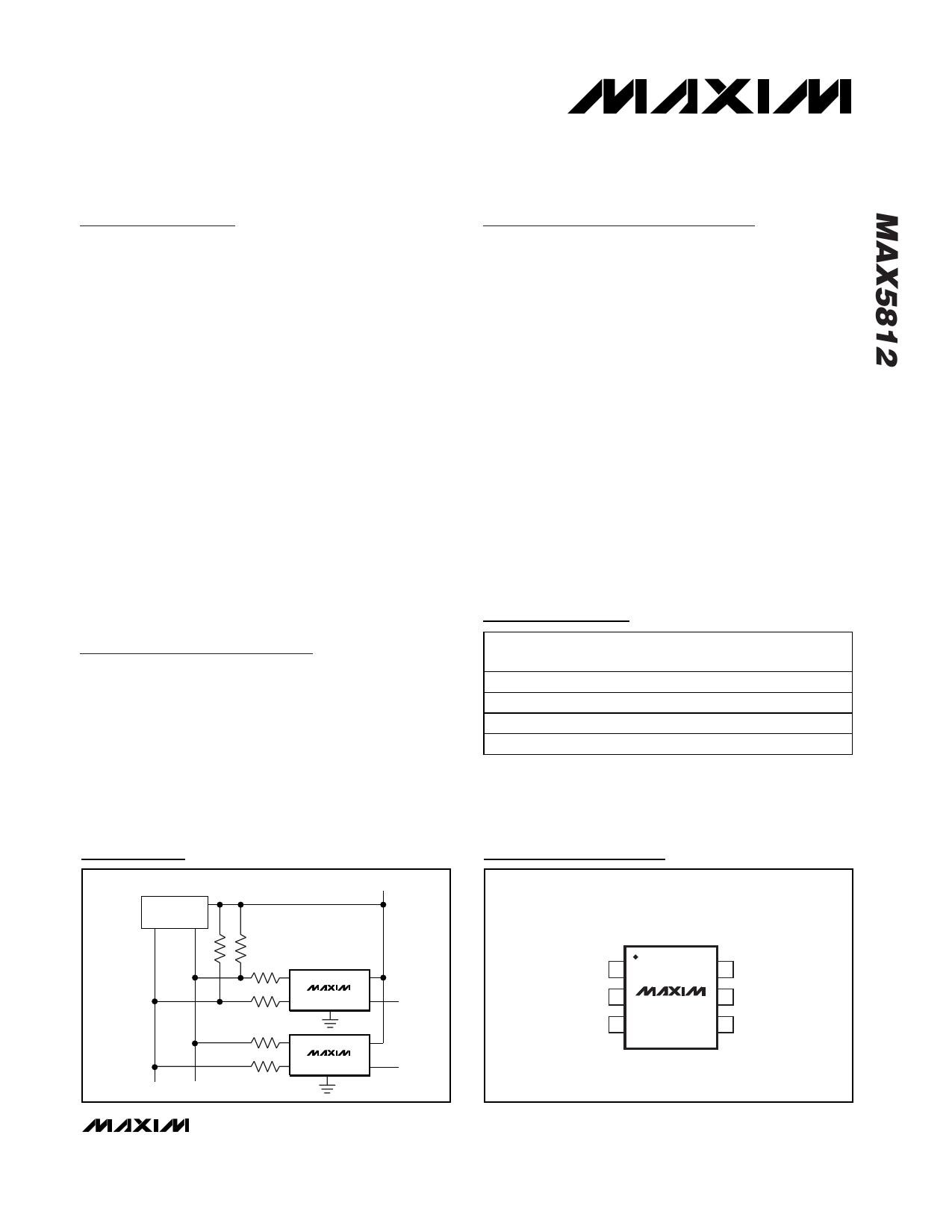
Pin Configuration
TOP VIEW
VDD 1
GND 2
SDA 3
MAX5812
6 OUT
5 ADD
4 SCL
SOT23
________________________________________________________________ Maxim Integrated Products 1
For pricing, delivery, and ordering information, please contact Maxim/Dallas Direct! at
1-888-629-4642, or visit Maxim’s website at www.maxim-ic.com.
1 page 
12-Bit Low-Power, 2-Wire, Serial
Voltage-Output DAC
(VDD = +5V, RL = 5kΩ, TA = +25°C.)
GAIN ERROR vs. TEMPERATURE
-2.0
-1.6
-1.2
-0.8
-0.4
0
-40
120
NO LOAD
-15 10 35 60
TEMPERATURE (°C)
SUPPLY CURRENT
vs. INPUT CODE
85
Typical Operating Characteristics (continued)
DAC OUTPUT VOLTAGE
vs. OUTPUT SOURCE CURRENT (NOTE 6)
6
5
4
3
2
1
CODE = FFF hex
0
0 24 68
OUTPUT SOURCE CURRENT (mA)
SUPPLY CURRENT
vs. TEMPERATURE
100
10
DAC OUTPUT VOLTAGE
vs. OUTPUT SINK CURRENT (NOTE 6)
2.5
2.0
1.5
CODE = 400 hex
1.0
0.5
0
0
100
24 68
OUTPUT SINK CURRENT (mA)
SUPPLY CURRENT
vs. SUPPLY VOLTAGE
10
100
80
60
40
20
NO LOAD
0
0 819
1638 2457
INPUT CODE
3276 4096
POWER-DOWN SUPPLY CURRENT
vs. SUPPLY VOLTAGE
500
95
90
85
NO LOAD
CODE = FFF hex
80
-40
-15 10
35
TEMPERATURE (°C)
60
85
POWER-UP GLITCH
MAX5812 toc17
90
80
70
60
50
2.7
CODE = FFF hex
NO LOAD
3.4 4.1 4.8
SUPPLY VOLTAGE (V)
5.5
EXITING SHUTDOWN
MAX5812 toc18
400
300 TA = -40°C
TA = +25°C
200
100
0
2.7
TA = +85°C
ZOUT = HIGH IMPEDANCE
NO LOAD
3.4 4.1 4.8
SUPPLY VOLTAGE (V)
5.5
VDD
OUT
100µs/div
Note 6: The ability to drive loads less than 5kΩ is not implied.
5V
0 OUT
10mV/div
500mV/div
CLOAD = 200pF
2µs/div
CODE = 800 hex
_______________________________________________________________________________________ 5
5 Page 
12-Bit Low-Power, 2-Wire, Serial
Voltage-Output DAC
MSB LSB MSB
S
A6
A5
A4
A3
A2
A1
A0
R/W
=0
ACK
C3 C2 X
XX
LSB
X X X ACK
DATA BYTES GENERATED BY MASTER DEVICE
MSB LSB
Sr
A6
A5
A4
A3
A2
A1
A0
R/W
=1
ACK
MSB LSB
X X PD1 PD0 D11 D10 D9 D8
ACK
DATA BYTES GENERATED BY MAX5812
MSB
D7 D6 D5 D4 D3 D2
LSB
D1 D0
ACK
Figure 7. Example Read Word Data Sequence
P
ACK GENERATED BY
MASTER DEVICE
IN OUT
MAX6030/
MAX6050
GND
VDD
MAX5812
GND
OUT
Figure 8. Powering the MAX5812 from An External Reference
Read Data Format
In read mode (R/W = 1), the MAX5812 writes the con-
tents of the DAC register to the bus. The direction of
data flow reverses after the address acknowledge by
the MAX5812. The device transmits the first byte of
data, waits for the master to acknowledge, and then
transmits the second byte. Figure 7 shows an example-
read data sequence.
I2C Compatibility
The MAX5812 is compatible with existing I2C systems.
SCL and SDA are high-impedance inputs; SDA has an
open drain that pulls the data line low during the ninth
clock pulse. The Typical Operating Circuit shows a typ-
ical I2C application. The communication protocol sup-
ports standard I2C 8-bit communications. The general
call address is ignored. The MAX5812 address is com-
patible only with the 7-bit I2C addressing protocol. Ten-
bit address formats are not supported.
Digital Feedthrough Suppression
When the MAX5812 detects an address mismatch, the
serial interface disconnects the SCL signal from the
core circuitry. This minimizes digital feedthrough
caused by the SCL signal on a static output. The serial
interface reconnects the SCL signal when a valid
START condition is detected.
Applications Information
Powering the Device From an
External Reference
The MAX5812 uses the VDD as the DAC voltage refer-
ence. Any power-supply noise is directly coupled to the
device output. The circuit in Figure 8 uses a precision
voltage reference to power the MAX5812, isolating the
device from any power-supply noise. Powering the
MAX5812 in such a manner greatly improves overall
performance, especially in noisy systems. The
MAX6030 (3V, 75ppm/°C) or the MAX6050 (5V,
75ppm/°C) precision voltage references are ideal
choices because of the low power requirements of the
MAX5812.
Digital Inputs and Interface Logic
The MAX5812 2-wire digital interface is I2C and SMBus-
compatible. The two digital inputs (SCL and SDA) load
______________________________________________________________________________________ 11
11 Page | ||
| Páginas | Total 13 Páginas | |
| PDF Descargar | [ Datasheet MAX5812.PDF ] | |
Hoja de datos destacado
| Número de pieza | Descripción | Fabricantes |
| MAX5811 | 10-Bit / Low-Power / 2-Wire Interface / Serial / Voltage-Output DAC | Maxim Integrated |
| MAX5812 | 12-Bit Low-Power / 2-Wire / Serial Voltage-Output DAC | Maxim Integrated |
| MAX5813 | Ultra-Small Quad-Channel 8-/10-/12-Bit Buffered Output DACs | Maxim Integrated Products |
| MAX5814 | Ultra-Small Quad-Channel 8-/10-/12-Bit Buffered Output DACs | Maxim Integrated Products |
| Número de pieza | Descripción | Fabricantes |
| SLA6805M | High Voltage 3 phase Motor Driver IC. |
Sanken |
| SDC1742 | 12- and 14-Bit Hybrid Synchro / Resolver-to-Digital Converters. |
Analog Devices |
|
DataSheet.es es una pagina web que funciona como un repositorio de manuales o hoja de datos de muchos de los productos más populares, |
| DataSheet.es | 2020 | Privacy Policy | Contacto | Buscar |