|
|
PDF MC-4532CD647PF-A75 Data sheet ( Hoja de datos )
| Número de pieza | MC-4532CD647PF-A75 | |
| Descripción | 32M-WORD BY 64-BIT SYNCHRONOUS DYNAMIC RAM MODULE UNBUFFERED TYPE | |
| Fabricantes | NEC | |
| Logotipo |  |
|
Hay una vista previa y un enlace de descarga de MC-4532CD647PF-A75 (archivo pdf) en la parte inferior de esta página. Total 16 Páginas | ||
|
No Preview Available !
DATA SHEET
MOS INTEGRATED CIRCUIT
MC-4532CD647
32M-WORD BY 64-BIT SYNCHRONOUS DYNAMIC RAM MODULE
UNBUFFERED TYPE
5 Description
The MC-4532CD647EF and MC-4532CD647PF are 33,554,432 words by 64 bits synchronous dynamic RAM
module on which 16 pieces of 128M SDRAM: µPD45128841 are assembled.
This module provides high density and large quantities of memory in a small space without utilizing the surface-
mounting technology on the printed circuit board.
Decoupling capacitors are mounted on power supply line for noise reduction.
Features
• 33,554,432 words by 64 bits organization
• Clock frequency and access time from CLK.
Part number
/CAS latency
Clock frequency
(MAX.)
Access time from CLK
(MAX.)
MC-4532CD647EF-A75
5
5 MC-4532CD647PF-A75
5
CL = 3
CL = 2
CL = 3
CL = 2
133 MHz
100 MHz
133 MHz
100 MHz
5.4 ns
6.0 ns
5.4 ns
6.0 ns
• Fully Synchronous Dynamic RAM, with all signals referenced to a positive clock edge
• Pulsed interface
• Possible to assert random column address in every cycle
• Quad internal banks controlled by BA0 and BA1 (Bank Select)
• Programmable burst-length (1, 2, 4, 8 and full page)
• Programmable wrap sequence (Sequential / Interleave)
5 • Programmable /CAS latency (2, 3)
• Automatic precharge and controlled precharge
• CBR (Auto) refresh and self refresh
• All DQs have 10 Ω ±10 % of series resistor
• Single 3.3 V ± 0.3 V power supply
• LVTTL compatible
• 4,096 refresh cycles/64 ms
• Burst termination by Burst Stop command and Precharge command
• 168-pin dual in-line memory module (Pin pitch = 1.27 mm)
• Unbuffered type
• Serial PD
The information in this document is subject to change without notice. Before using this document, please
confirm that this is the latest version.
Not all devices/types available in every country. Please check with local NEC representative for
availability and additional information.
Document No. M14276EJ2V0DS00 (2nd edition)
Date Published January 2000 NS CP(K)
Printed in Japan
The mark • shows major revised points.
©
1999
1 page 
MC-4532CD647
Electrical Specifications
• All voltages are referenced to VSS (GND).
• After power up, wait more than 100 µs and then, execute power on sequence and CBR (Auto) refresh before proper
device operation is achieved.
Absolute Maximum Ratings
Parameter
Symbol
Voltage on power supply pin relative to GND VCC
Voltage on input pin relative to GND
VT
Short circuit output current
IO
Power dissipation
PD
Operating ambient temperature
TA
Storage temperature
Tstg
Condition
Rating
–0.5 to +4.6
–0.5 to +4.6
50
16
0 to 70
–55 to +125
Unit
V
V
mA
W
°C
°C
Caution Exposing the device to stress above those listed in Absolute Maximum Ratings could cause
permanent damage. The device is not meant to be operated under conditions outside the limits
described in the operational section of this specification. Exposure to Absolute Maximum Rating
conditions for extended periods may affect device reliability.
Recommended Operating Conditions
Parameter
Supply voltage
High level input voltage
Low level input voltage
Operating ambient temperature
Symbol
VCC
VIH
VIL
TA
Condition
MIN.
3.0
2.0
−0.3
0
TYP.
3.3
MAX.
3.6
VCC + 0.3
+0.8
70
Unit
V
V
V
°C
Capacitance (TA = 25 °C, f = 1 MHz)
Parameter
Input capacitance
Data input/output capacitance
Symbol
Test condition
CI1 A0 - A11, BA0 (A13), BA1 (A12),
/RAS, /CAS, /WE
CI2 CLK0 - CLK3
CI3 CKE0, CKE1
CI4 /CS0 - /CS3
CI5 DQMB0 - DQMB7
CI/O DQ0 - DQ63
MIN.
58
24
32
17
10
11
TYP.
MAX.
94
40
52
29
17
19
Unit
pF
pF
Data Sheet M14276EJ2V0DS00
5
5 Page 
MC-4532CD647
(2/2)
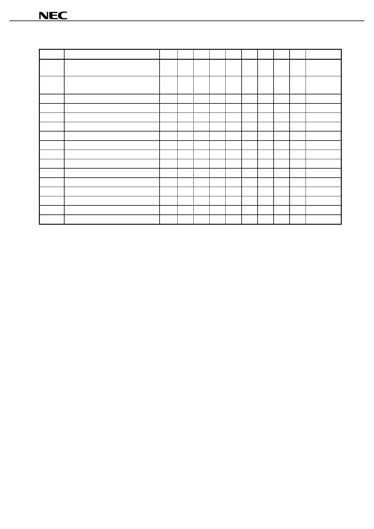
Byte No.
Function Described
Hex Bit 7 Bit 6 Bit 5 Bit 4 Bit 3 Bit 2 Bit 1 Bit 0
Notes
32 Command and address signal input
setup time
15H 0 0 0 1 0 1 0 1 1.5 ns
33 Command and address signal input
08H 0 0 0 0 1 0 0 0 0.8 ns
hold time
34 Data signal input setup time
15H 0 0 0 1 0 1 0 1 1.5 ns
35 Data signal input hold time
08H 0 0 0 0 1 0 0 0 0.8 ns
36-61
00H 0 0 0 0 0 0 0 0
5 62 SPD revision
5 63 Checksum for bytes 0 - 62
12H 0 0 0 1 0 0 1 0 1.2
B0H 1 0 1 1 0 0 0 0
64-71 Manufacture’s JEDEC ID code
72 Manufacturing location
73-90 Manufacture’s P/N
91-92 Revision code
93-94 Manufacturing date
95-98 Assembly serial number
99-125 Mfg specific
126 Intel specification frequency
64H 0 1 1 0 0 1 0 0
127 Intel specification /CAS latency support FDH 1 1 1 1 1 1 0 1
Timing Chart
Refer to the SYNCHORONOUS DRAM MODULE TIMING CHART Information (M13348E).
Data Sheet M14276EJ2V0DS00
11
11 Page | ||
| Páginas | Total 16 Páginas | |
| PDF Descargar | [ Datasheet MC-4532CD647PF-A75.PDF ] | |
Hoja de datos destacado
| Número de pieza | Descripción | Fabricantes |
| MC-4532CD647PF-A75 | 32M-WORD BY 64-BIT SYNCHRONOUS DYNAMIC RAM MODULE UNBUFFERED TYPE | NEC |
| Número de pieza | Descripción | Fabricantes |
| SLA6805M | High Voltage 3 phase Motor Driver IC. |
Sanken |
| SDC1742 | 12- and 14-Bit Hybrid Synchro / Resolver-to-Digital Converters. |
Analog Devices |
|
DataSheet.es es una pagina web que funciona como un repositorio de manuales o hoja de datos de muchos de los productos más populares, |
| DataSheet.es | 2020 | Privacy Policy | Contacto | Buscar |
