|
|
PDF LR38269 Data sheet ( Hoja de datos )
| Número de pieza | LR38269 | |
| Descripción | Digital Signal Processor for Color CCD Cameras | |
| Fabricantes | Sharp | |
| Logotipo |  |
|
Hay una vista previa y un enlace de descarga de LR38269 (archivo pdf) en la parte inferior de esta página. Total 20 Páginas | ||
|
No Preview Available !
LR38269
DESCRIPTION
The LR38269 is a CMOS digital signal processor
for color CCD camera system of 270 k/320 k-pixel
CCD with complementary color filters. The camera
system consists of CDS/AGC/ADC IC (IR3Y38M),
DSP IC (LR38269), and V driver IC (LR36685) with
CCD.
FEATURES
• Designed for 270 k/320 k color CCDs with Mg, G,
Cy, and Ye complementary color filters
• Switchable between NTSC and PAL modes
• External control interface input/output
• Variable GAMMA and KNEE response
(Select one out of 4 kinds of GAMMA & KNEE
response)
• 10-bit digital input
• Analog NTSC/PAL composite output by built-in 9-
bit 1 ch DA converter
• Built-in mirror image function
• Built-in timing generator to drive CCD
• Built-in 2 k-bit EEPROM controller to set the
camera adjustment data
• Built-in auto exposure control
• Built-in auto white balance control
• Built-in auto carrier balance control
• Single + 3.3 V power supply
• Package :
80-pin LQFP (LQFP080-P-1212) 0.5 mm pin-pitch
LR38269
Digital Signal Processor for
Color CCD Cameras
In the absence of confirmation by device specification sheets, SHARP takes no responsibility for any defects that may occur in equipment using any SHARP devices shown in
catalogs, data books, etc. Contact SHARP in order to obtain the latest device specification sheets before using any SHARP device.
1
1 page 
LR38269
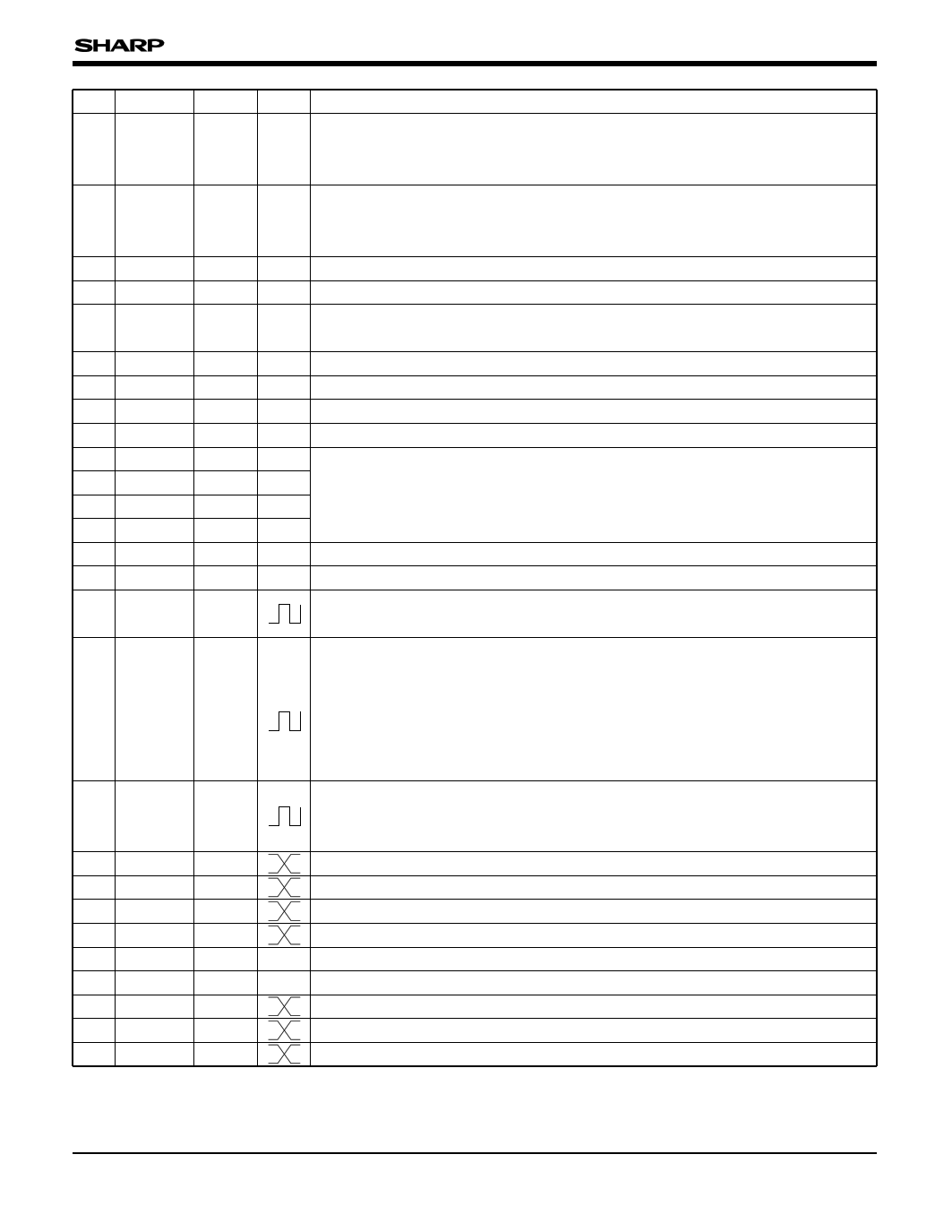
PIN NO. SYMBOL I/O POLARITY
DESCRIPTION
Video output mode setting.
32 MIR
IO4M
L : Normal
H : Mirror
In digital output mode, this pin is assigned to bit 2 of U/V signal.
Backlight compensation selection.
33 BLC
IO4M
L : OFF
H : ON
In digital output mode, this pin is assigned to bit 3 of U/V signal.
34 GNDDA
–
A grounding pin of built-in DA converter.
35 VDDDA
–
Supply of +3.3 V power of built-in DA converter.
36 VB
DAO
Bias voltage output of built-in DA converter, connected to GND through a
capacitor.
37 IREF
DAO
Bias current output of built-in DA converter, connected to GND through a resistor.
38 VREF
DAI
Bias voltage input of built-in DA converter, connected to +1.0 V power supply.
39 GNDDA
–
A grounding pin of built-in DA converter.
40 VIDEO DAO
Analog video signal output.
41 EEMDS IO4MU
Electronic exposure mode setting by EEMDS, EEMD1, EEMD2 and EEMD3.
42 EEMD1 IO4MU
See "Electronic Shutter Speed Setting" in AUTOMATIC CAMERA FUNCTION
43 EEMD2 IO4MU
CONTROL.
44 EEMD3 IO4MU
In digital output mode, 41 to 44 pins are assigned to bits 7 to 4 of U/V signals.
45 GND
–
A grounding pin
46 VDD
–
Supply of +3.3 V power.
47 DCK1
OBF4M
Clock output for digital signal output.
Output mode setting switches to CSYNC output.
ID pulse output for U/V output signal. In digital output, this pin outputs KEI-
PULSE.
48 DCK2
OBF4M
49 EXCKI
IC
50 Y0
51 Y1
52 Y2
53 Y3
54 GND
55 VDD
56 Y4
57 Y5
58 Y6
OBF4M
OBF4M
OBF4M
OBF4M
–
–
OBF4M
OBF4M
OBF4M
NOTE : KEI-PULSE
At power-on, it keeps low. Both 1/60 s (PAL 1/50 s) as shutter speed and AGC gain
more than data of address 78h sets it high.
Bit 3 of address 03h sets the function of this pin.
1 : Clock input of 13.5 MHz for digital output
0 : VRI input for analog output
Bit 0 (LSB) of digital luminance signal output.
Bit 1 of digital luminance signal output.
Bit 2 of digital luminance signal output.
Bit 3 of digital luminance signal output.
A grounding pin.
Supply of +3.3 V power.
Bit 4 of digital luminance signal output.
Bit 5 of digital luminance signal output.
Bit 6 of digital luminance signal output.
5
5 Page 
LR38269
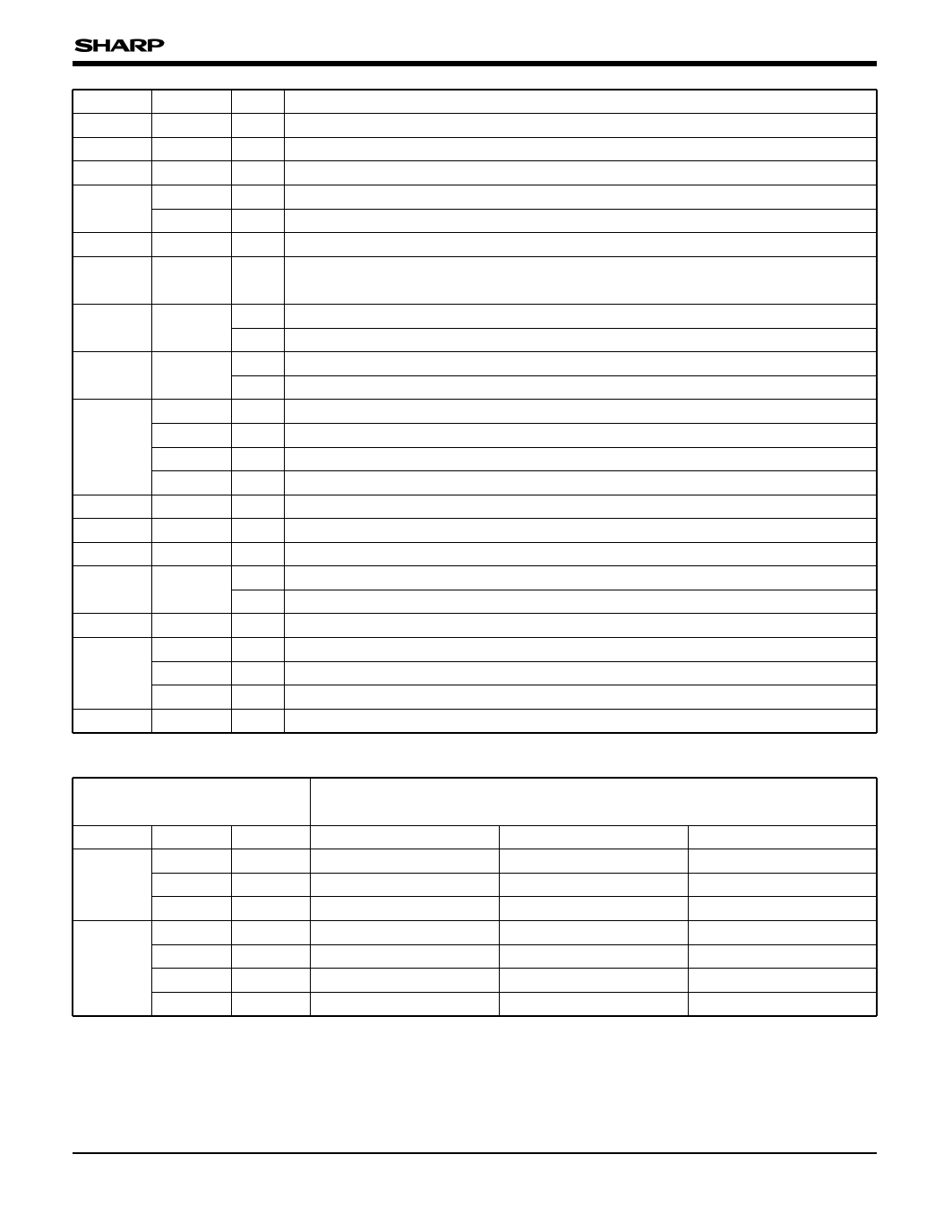
ADDRESS NAME
69h APT_HCL
6Ah APT_VGA
6Bh APT_VCL
6Ch CBLK_LV
SETUP
6Dh VARI_Y
6Eh
SW_CTRL
BIT
6-0
4-0
6-0
7
6-1
4-0
7-0
6Fh 7-5
TG_SEL1
4-2
70h 7-5
TG_SEL2
4-2
71h ENC_MUTE 7
SYNC_SW 6
SEL_RB 5
OUT_GAIN 4-0
72h SYNC_LEV 7-0
73h BAS_R 7-0
74h BAS_B 7-0
75h 7
MUTE_OUT
6-0
76h TEST
2-0
77h VRI
2
TEST
1
TEST
0
78h KEI_AGC 8
CONTENTS
Horizontal aperture signal coring
Vertical aperture gain
Vertical aperture signal coring
CBLK level selection
0 : 00h
1 : 10h
Set up level
luminance signal position
The following setting is available under both EEPSL = H and digital output mode
WB1 (LSB), WB2, BACK, EEMDS, EEMD1 EEMD2, EEMD3, MIR (MSB)
ADCK phase setting (6 steps per 60˚)
FS phase setting (±2 ns x 3)
FCDS phase setting (±2 ns x 3)
FR phase setting (±2 ns x 3)
Encoder muting
0 : OFF
1 : ON
SYNC adder
0 : ON
1 : OFF
Serial digital data setting
Gain of video output amplifier
SYNC level (80h = 40 IRE)
BURST level of R – Y
BURST level of B – Y
Muting at power-on
Muting period (data multiplied by 1 field period)
Test data (EEPROM data must be 00h)
EXCKI pin function
1 : VRI function 0 : Clock input
Test data (EEPROM data must be 0)
Test data (EEPROM data must be 0)
AGC gain to set KEI-PULSE high
(NOTE 1)
ADDRESS
01
Bit 3
Bit 2
DIGITAL
1
10
x
ANALOG
1
00
1
0
Bit 0
0
0
1
0
0
1
1
DCK1 (Pin 47)
DCK1
DCK1
DCK1
CSYNC
CSYNC
CSYNC
CSYNC
SIGNAL OUTPUT
VD (Pin 61)
VD for video out
VD for CCD driving
CSYNC
VD for video out
VD for CCD driving
VD for video out
VD for CCD driving
HD (Pin 60)
HD
HD
HD
HD
HD
BELL
BELL
11
11 Page | ||
| Páginas | Total 20 Páginas | |
| PDF Descargar | [ Datasheet LR38269.PDF ] | |
Hoja de datos destacado
| Número de pieza | Descripción | Fabricantes |
| LR38266 | Digital Signal Processor for Color CCD Cameras | Sharp |
| LR38269 | Digital Signal Processor for Color CCD Cameras | Sharp |
| Número de pieza | Descripción | Fabricantes |
| SLA6805M | High Voltage 3 phase Motor Driver IC. |
Sanken |
| SDC1742 | 12- and 14-Bit Hybrid Synchro / Resolver-to-Digital Converters. |
Analog Devices |
|
DataSheet.es es una pagina web que funciona como un repositorio de manuales o hoja de datos de muchos de los productos más populares, |
| DataSheet.es | 2020 | Privacy Policy | Contacto | Buscar |
