|
|
PDF VV6501 Data sheet ( Hoja de datos )
| Número de pieza | VV6501 | |
| Descripción | DUAL-MODE DIGITAL CAMERA CO-PROCESSOR | |
| Fabricantes | STMicroelectronics | |
| Logotipo |  |
|
Hay una vista previa y un enlace de descarga de VV6501 (archivo pdf) en la parte inferior de esta página. Total 30 Páginas | ||
|
No Preview Available !
www.DataSheet4U.com
® VV6501
VGA CMOS Color Image Sensor
Features
s 640 x 480 VGA resolution
s 1/4 inch format lens compatible
s On board 10 bit ADC
s On board voltage regulators
s Automatic dark calibration
s On board audio amplifier
s I2C interface
s Low power suspend mode
s 4 or 5 wire nibble output
s Framegrabber signals: QCK and FST
Description
This image sensor based on STMicroelectronics
CMOS technology is Bayer colorised.
The sensor provides a raw digital video output
which also contains embedded codes to facilitate
external synchronisation.
The sensor interfaces to a range of
STMicroelectronics companion processors for
applications such as USB webcams and digital stills
cameras.
An I2C interface allows an external processor to
configure the device and control exposure and gain
settings.
A low-power pin-driven suspend mode simplifies
USB-based designs.
On board voltage regulators operate from a 5V
USB supply and generate 3V3 and 1V8 power
supplies for external processors.
Technical Specifications
Image Size
Pixel size
Array size
Analogue gain
Sensitivity (typ.)
Maximum frame rate
Supply voltage
Power consumption
Operating temperature
Package type
640 x 480 (VGA)
5.6 µm x 5.6 µm
3.6 mm x 2.7 mm
x1 to x16
2.05 V/lux-sec
30 fps (with 24MHz clock)
5V (USB)
3V3 direct drive
Active (30fps)
< 30 mA
Suspend
< 100 µA
0oC - 40oC
36 pin CLCC
Ordering Details
Part Number
VV6501C001
Description
36pin CLCC, colorised sensor
September 2003
1/60
1 page 
VV6501
Overview
1.2 Typical application
1.2.1
USB webcam
This sensor may be used in conjunction with the STMicroelectronics STV0676 co-processor to
produce a low cost USB webcam.
In this application the co-processor supplies the sensor clock and uses the embedded control
sequences to synchronise with the frame and line level timings. It then performs the colour
processing on the raw image data from the sensor before supplying the final image data to the host
using the USB interface.
The voltage regulators on-board the sensor are used to control external bipolar transistors to derive
the supplies for the sensor and co-processor from the 5V USB supply. This approach eliminates the
requirement for more costly external voltage regulation circuitry.
Figure 2 below illustrates a typical system using VV6501.
Figure 2: USB camera system using STV0676
USB
Hub
USB-power
USB - data
V5V
GND
USB Webcam
VV6501
Power management
Digital interface
3V3
1V8
I2C
suspend
VGA pixel array
video D[4:0]
STV0676
Co-processor
Video
processing
Microphone
Audio amplifier
USB
interface
The input USB supply is 5 V. The 3V3 digital regulator generates the supply for the sensor digital
part and the co-processor IOs. The 1V8 regulator generates the core supply for the co-processor.
5/60
5 Page 
VV6501
Functional Description
3.1.4
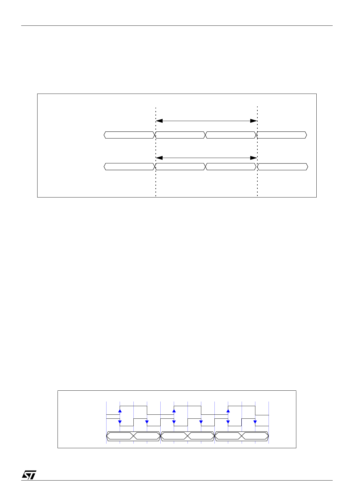
Digital data bus: D[4:0]
Sensor data may be either 8 or 10 bits per pixel and is transmitted as follows:
q 10-bit data: A pair of 5-bit nibbles, most significant nibble first, on 5 wires.
q 8-bit data: A pair of 4-bit nibbles, most significant nibble first, on 4 wires.
Figure 6: Digital data output modes
5-wire output mode
D4,D3,D2,D1,D0
4-wire output mode
D3,D2,D1,D0
10-bit pixel data
D9,D8,D7,D6,D5
D4,D3,D2,D1,D0
8-bit pixel data
D7,D6,D5,D4
D3,D2,D1,D0
D9,D8,D7,D6,D5
D7,D6,D5,D4
In 5-wire mode, the embedded control codes occupy only the most significant 8-bits, the least
significant 2-bits are always zero.
Output tri-state using SIF
Register 23 bit[5] can be used to tri-state all 5 data lines, QCK and FST.
Output pad drive strength
The data and QCK output pads are tri-stateable with 4 mA drive.
3.1.5
Data qualification clock (QCK)
A data qualification clock (QCK) is available and complements the embedded control sequences.
This clock runs continuously when enabled and consists of:
q Fast QCK: the falling edge of the clock qualifies every 5 or 4-bit data blocks that constitute a
pixel value.
q Slow QCK: the rising edge qualifies 1st, 3rd, 5th, etc. blocks of data that constitute a pixel
value while the falling edge qualifies the 2nd, 4th, 6th etc. blocks of data. For example in 4-wire
mode, the rising edge of the clock qualifies the most significant nibbles while the falling edge of
the clock qualifies the least significant nibbles.
Figure 7: QCK modes
QCK (slow)
QCK (fast)
D[4:0] <MSB> <LSB> <MSB> <LSB> <MSB> <LSB>
11/60
11 Page | ||
| Páginas | Total 30 Páginas | |
| PDF Descargar | [ Datasheet VV6501.PDF ] | |
Hoja de datos destacado
| Número de pieza | Descripción | Fabricantes |
| VV6500 | DUAL-MODE DIGITAL CAMERA CHIPSET | STMicroelectronics |
| VV6500C001 | DUAL-MODE DIGITAL CAMERA CHIPSET | STMicroelectronics |
| VV6501 | DUAL-MODE DIGITAL CAMERA CO-PROCESSOR | STMicroelectronics |
| VV6501C001 | DUAL-MODE DIGITAL CAMERA CO-PROCESSOR | STMicroelectronics |
| Número de pieza | Descripción | Fabricantes |
| SLA6805M | High Voltage 3 phase Motor Driver IC. |
Sanken |
| SDC1742 | 12- and 14-Bit Hybrid Synchro / Resolver-to-Digital Converters. |
Analog Devices |
|
DataSheet.es es una pagina web que funciona como un repositorio de manuales o hoja de datos de muchos de los productos más populares, |
| DataSheet.es | 2020 | Privacy Policy | Contacto | Buscar |
