|
|
|
PDF IL55B Data sheet ( Hoja de datos )
| Número de pieza | IL55B | |
| Descripción | PHOTODARLINGTON OPTOCOUPLER | |
| Fabricantes | Siemens Semiconductor Group | |
| Logotipo | ||
 1. - Photodarlington Optocoupler - Siemens Hay una vista previa y un enlace de descarga de IL55B (archivo pdf) en la parte inferior de esta página. Total 2 Páginas | ||
|
No Preview Available !
IL55B
PHOTODARLINGTON
OPTOCOUPLER
FEATURES
• High Collector-Emitter Breakdown Voltage—
80 V minimum
• High Isolation Resistance, 1011 W Typical
• Standard Plastic DIP Package
• Underwriters Lab File #E52744
•
V
DE
VDE 0884 Available with Option 1
DESCRIPTION
The IL55B is an optically coupled isolator with a Gal-
lium Arsenide infrared LED and a silicon photodarling-
ton sensor. Switching can be achieved while
maintaining a high degree of isolation between driving
and load circuits. These optocouplers can be used to
replace reed and mercury relays with advantages of
long life, high speed switching and elimination of
magnetic fields.
Maximum Ratings
Emitter
Peak Reverse Voltage ............................................. 3 V
Continuous Forward Current .............................. 60 mA
Power Dissipation at 25°C............................... 100 mW
Derate Linearly from 55°C ......................... 1.33 mW/°C
Detector
Collector-Emitter Breakdown Voltage, BVCEO....... 80 V
Emitter-Collector Breakdown Voltage BVECO.......... 5 V
Collector (load) Current.................................... 125 mA
Power Dissipation at 25°C Ambient ................ 150 mW
Derate Linearly from 25°C ........................... 2.0 mW/°C
Package
Total Dissipation at 25°C Ambient .................. 250 mW
Derate Linearly from 25°C ........................... 3.3 mW/°C
Isolation Test Voltage (between
emitter and detector refered to
standard climate 23°C/50%RH,
DIN 50014) ......................................... 5300 VACRMS
Creepage ................................................... 7 mm min.
Clearance.................................................... 7 mm min.
Tracking Resitance, Group III
(KC>600 per VDE 110 § 6,Table 3
and DIN 53480/VDE 0330, Part 1
Isolation Resistance
VIO=500 V, TA=25°C .......................................1012 Ω
VIO=500 V, TA=100°C .....................................1011 Ω
Storage Temperature ........................ –55°C to +150°C
Operating Temperature .................... –55°C to +100°C
Lead Soldering Time at 260°C ......................... 10 sec.
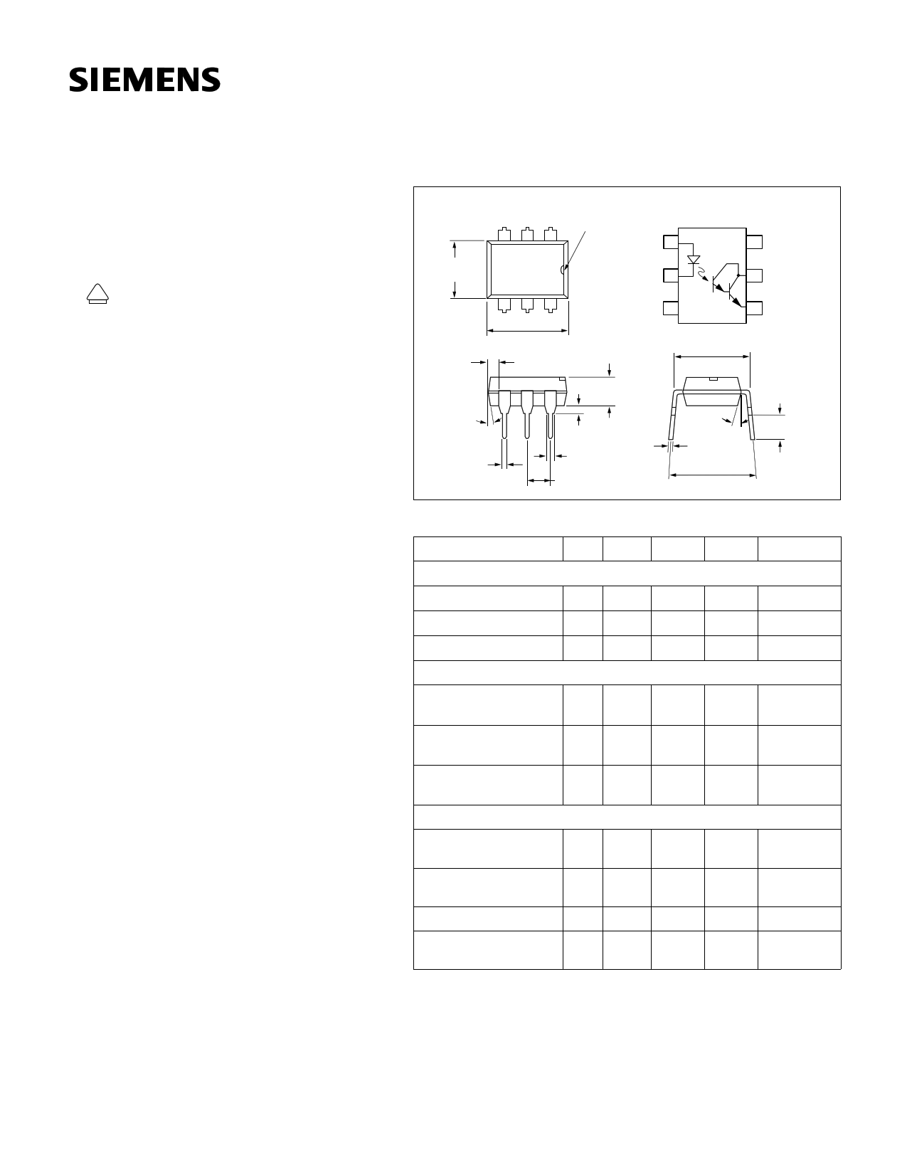
Package Dimensions in Inches (mm)
Pin One ID.
321
Anode 1
.248 (6.30)
.256 (6.50)
Cathode 2
6 Base
5 Collector
.039
(1.00)
min.
4°
typ.
.018 (0.45)
.022 (0.55)
4 56
.335 (8.50)
.343 (8.70)
NC 3
.300 (7.62)
typ.
.130 (3.30)
.150 (3.81)
.020 (.051) min.
.031 (0.80)
.035 (0.90)
.100 (2.54) typ.
18° typ.
.010 (.25)
.014 (.35)
.300 (7.62)
.347 (8.82)
4 Emitter
.110 (2.79)
.150 (3.81)
Electrical Characteristics (TA=25°C)
Parameter
Min. Typ.
Emitter
Forward Voltage*
1.25
Reverse Current*
0.1
Capacitance
25
Detector
BVCEO
80
Max.
1.5
10
Unit
V
µA
pF
V
BVECO
5 10
V
ICEO
1 µA
Package
Current Transfer
Ratio
Coupling
Capacitance
Turn-On Time
Turn -Off Time
500
1.5
5
100
%
pF
µs
µs
Condition
IF=50 mA
VR=3.0 V
VR=0 V
IC=1 mA,
IF=0
IE=100 µA,
IF=0
VCE=60 V,
IF=0
IF=10 mA
VCE =1.5 V
VCC=10 V
IF=5 mA
RL=100 Ω
5–1
1 page | ||
| Páginas | Total 2 Páginas | |
| PDF Descargar | [ Datasheet IL55B.PDF ] | |
Hoja de datos destacado
| Número de pieza | Descripción | Fabricantes |
| IL55 | PHOTODARLINGTON OPTOCOUPLER | Siemens Semiconductor Group |
| IL55B | PHOTODARLINGTON OPTOCOUPLER | Siemens Semiconductor Group |
| IL55B | (IL55B / IL56B) Optocoupler / Photodarlington Output / High Gain | Vishay Siliconix |
| Número de pieza | Descripción | Fabricantes |
| SLA6805M | High Voltage 3 phase Motor Driver IC. |
Sanken |
| SDC1742 | 12- and 14-Bit Hybrid Synchro / Resolver-to-Digital Converters. |
Analog Devices |
|
DataSheet.es es una pagina web que funciona como un repositorio de manuales o hoja de datos de muchos de los productos más populares, |
| DataSheet.es | 2020 | Privacy Policy | Contacto | Buscar |