|
|
|
PDF 4X16E43V Data sheet ( Hoja de datos )
| Número de pieza | 4X16E43V | |
| Descripción | 4 MEG x 16 EDO DRAM | |
| Fabricantes | ETC | |
| Logotipo | ||
Hay una vista previa y un enlace de descarga de 4X16E43V (archivo pdf) en la parte inferior de esta página. Total 24 Páginas | ||
|
No Preview Available !
EDO DRAM
4 MEG x 16
EDO DRAM
4X16E43V
FEATURES
• Single +3.3V ±0.3V power supply
• Industry-standard x16 pinout, timing, functions,
and package
• 12 row, 10 column addresses (4)
13 row, 9 column addresses (8)
• High-performance CMOS silicon-gate process
• All inputs, outputs and clocks are LVTTL-compatible
• Extended Data-Out (EDO) PAGE MODE access
• 4,096-cycle CAS#-BEFORE-RAS# (CBR) REFRESH
distributed across 64ms
• Self refresh for low-power data retention
OPTIONS
• Plastic Package
50-pin TSOP (400 mil)
• Timing
50ns access
60ns access
• Refresh Rates
4K
8K
MARKING
TW
-5
-6
4
8
• Operating Temperature Range
Commercial (0°C to +70°C)
Extended (-40°C to +85°C)
None
IT
NOTE: 1. The “#” symbol indicates signal is active LOW.
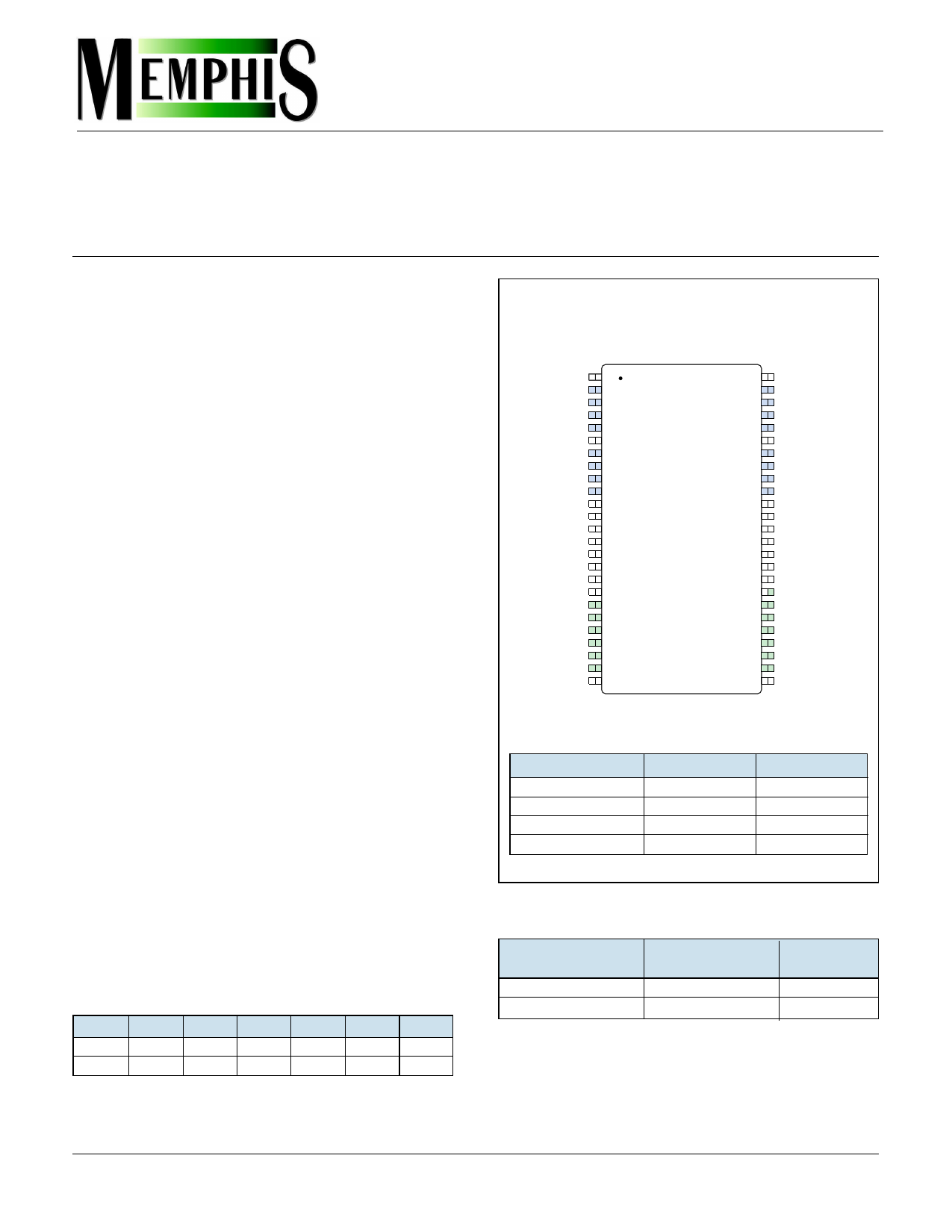
PIN ASSIGNMENT (Top View)
50-Pin TSOP
VCC
DQ0
DQ1
DQ2
DQ3
VCC
DQ4
DQ5
DQ6
DQ7
NC
VCC
WE#
RAS#
NC
NC
NC
NC
A0
A1
A2
A3
A4
A5
VCC
1
2
3
4
5
6
7
8
9
10
11
12
13
14
15
16
17
18
19
20
21
22
23
24
25
50 VSS
49 DQ15
48 DQ14
47 DQ13
46 DQ12
45 VSS
44 DQ11
43 DQ10
42 DQ9
41 DQ8
40 NC
39 VSS
38 CASL#
37 CASH#
36 OE#
35 NC
34 NC
33 NC/A12†
32 A11
31 A10
30 A9
29 A8
28 A7
27 A6
26 VSS
†A12 for "8K" version, NC for "4K" version.
Configuration
Refresh
Row Address
Column Addressing
4X16E43V
4 Meg x 16
4K
4K (A0-A11)
1K (A0-A9)
4X16E83V
4 Meg x 16
8K
8K (A0-A12)
512 (A0-A8)
Part Number Example:
MEM4X16E43VTW-5
KEY TIMING PARAMETERS
SPEED
-5
-6
tRC
84ns
104ns
tRAC
50ns
60ns
tPC
20ns
25ns
tAA
25ns
30ns
tCAC
13ns
15ns
tCAS
8ns
10ns
4 MEG x 16 EDO DRAM PART NUMBERS
PART NUMBER
4X16E43VTW-x
4X16E83VTW-x
x = speed
REFRESH
ADDRESSING
4
8
PACKAGE
400-TSOP
400-TSOP
1
1 page 
RAS#
V
V
IH
IL
CAS# VVIIHL
4 MEG x 16
EDO DRAM
ADDR
V
V
IH
IL
ROW
COLUMN (A)
COLUMN (B)
COLUMN (C)
COLUMN (D)
DQ
V
V
IOH
IOL
OE# VVIIHL
OPEN
VALID DATA (A)
tOD
tOES
tOE
VALID DATA (A)
VALID DATA (B)
tOD
tOEHC
VALID DATA (C)
tOD
tOEP
VALID DATA (D)
The DQs go back to
Low-Z if tOES is met.
The DQs remain High-Z
until the next CAS# cycle
if tOEHC is met.
Figure 3
OE# Control of DQs
The DQs remain High-Z
until the next CAS# cycle
if tOEP is met.
RAS# VVIIHL
CAS#
V
V
IH
IL
ADDR
V
V
IH
IL
DQ VVIIOOHL
WE#
V
V
IH
IL
OE#
V
V
IH
IL
ROW
COLUMN (A)
OPEN
VALID DATA (A)
tWHZ
tWPZ
COLUMN (B)
COLUMN (C)
VALID DATA (B)
tWHZ
INPUT DATA (C)
COLUMN (D)
The DQs go to High-Z if WE# falls and, if tWPZ is met,
will remain High-Z until CAS# goes LOW with
WE# HIGH (i.e., until a READ cycle is initiated).
Figure 4
WE# Control of DQs
WE# may be used to disable the DQs to prepare
for input data in an EARLY WRITE cycle. The DQs
will remain High-Z until CAS# goes LOW with
WE# HIGH (i.e., until a READ cycle is initiated).
DON?T CARE
UNDEFINED
5
5 Page 
NOTES
1. All voltages referenced to VSS.
2. This parameter is sampled. VCC = +3.3V; f = 1
MHz; TA = 25°C.
3. ICC is dependent on output loading and cycle
rates. Specified values are obtained with mini-
mum cycle time and the outputs open.
4. Enables on-chip refresh and address counters.
5. The minimum specifications are used only to
indicate cycle time at which proper operation
over the full temperature range is ensured.
6. An initial pause of 100µs is required after power-
up, followed by eight RAS# refresh cycles (RAS#-
ONLY or CBR with WE# HIGH), before proper
device operation is ensured. The eight RAS# cycle
wake-ups should be repeated any time the tREF
refresh requirement is exceeded.
7. AC characteristics assume tT = 2.5ns.
8. VIH (MIN) and VIL (MAX) are reference levels for
measuring timing of input signals. Transition
times are measured between VIH and VIL (or
between VIL and VIH).
9. In addition to meeting the transition rate
specification, all input signals must transit
between VIH and VIL (or between VIL and VIH) in a
monotonic manner.
10. If CAS# and RAS# = VIH, data output is High-Z.
11. If CAS# = VIL, data output may contain data from
the last valid READ cycle.
12. Measured with a load equivalent to two TTL
gates and 100pF; and VOL = 0.8V and VOH = 2V.
13. If CAS# is LOW at the falling edge of RAS#,
output data will be maintained from the previous
cycle. To initiate a new cycle and clear the data-
out buffer, CAS# must be pulsed HIGH for tCP.
14. The tRCD (MAX) limit is no longer specified.
tRCD (MAX) was specified as a reference point
only. If tRCD was greater than the specified tRCD
(MAX) limit, then access time was controlled
exclusively by tCAC (tRAC [MIN] no longer
applied). With or without the tRCD limit, tAA
and tCAC must always be met.
15. The tRAD (MAX) limit is no longer specified.
tRAD (MAX) was specified as a reference point
only. If tRAD was greater than the specified tRAD
(MAX) limit, then access time was controlled
exclusively by tAA (tRAC and tCAC no longer
applied). With or without the tRAD (MAX) limit,
tAA, tRAC, and tCAC must always be met.
4 MEG x 16
EEDDOODDRRAAMM
16. Either tRCH or tRRH must be satisfied for a READ
cycle.
17. tOFF (MAX) defines the time at which the output
achieves the open circuit condition and is not
referenced to VOH or VOL.
18. tWCS, tRWD, tAWD, and tCWD are not restrictive
operating parameters. tWCS applies to EARLY
WRITE cycles. If tWCS > tWCS (MIN), the cycle is
an EARLY WRITE cycle and the data output will
remain an open circuit throughout the entire
cycle. tRWD, tAWD, and tCWD define READ-
MODIFY-WRITE cycles. Meeting these limits
allows for reading and disabling output data and
then applying input data. OE# held HIGH and
WE# taken LOW after CAS# goes LOW results in a
LATE WRITE (OE#-controlled) cycle. tWCS, tRWD,
tCWD, and tAWD are not applicable in a LATE
WRITE cycle.
19. These parameters are referenced to CAS# leading
edge in EARLY WRITE cycles and WE# leading
edge in LATE WRITE or READ-MODIFY-WRITE
cycles.
20. If OE# is tied permanently LOW, LATE WRITE, or
READ-MODIFY-WRITE operations are not
possible.
21. A HIDDEN REFRESH may also be performed after
a WRITE cycle. In this case, WE# is LOW and
OE# is HIGH.
22. RAS#-ONLY REFRESH requires that all 8,192 rows
of the ARC8V4M16E or all 4,096 rows of the
4X16E43V be refreshed at least once every
64ms.
23. CBR REFRESH for either device requires that at
least 4,096 cycles be completed every 64ms.
24. The DQs go High-Z during READ cycles once tOD
or tOFF occur. If CAS# stays LOW while OE# is
brought HIGH, the DQs will go High-Z. If OE# is
brought back LOW (CAS# still LOW), the DQs
will provide the previously read data.
25. LATE WRITE and READ-MODIFY-WRITE cycles
must have both tOD and tOEH met (OE# HIGH
during WRITE cycle) in order to ensure that the
output buffers will be open during the WRITE
cycle. If OE# is taken back LOW while CAS#
remains LOW, the DQs will remain open.
26. Column address changed once each cycle.
27. The first CASx# edge to transition LOW.
11
11 Page | ||
| Páginas | Total 24 Páginas | |
| PDF Descargar | [ Datasheet 4X16E43V.PDF ] | |
Hoja de datos destacado
| Número de pieza | Descripción | Fabricantes |
| 4X16E43V | 4 MEG x 16 EDO DRAM | ETC |
| Número de pieza | Descripción | Fabricantes |
| SLA6805M | High Voltage 3 phase Motor Driver IC. |
Sanken |
| SDC1742 | 12- and 14-Bit Hybrid Synchro / Resolver-to-Digital Converters. |
Analog Devices |
|
DataSheet.es es una pagina web que funciona como un repositorio de manuales o hoja de datos de muchos de los productos más populares, |
| DataSheet.es | 2020 | Privacy Policy | Contacto | Buscar |