|
|
PDF FN6094 Data sheet ( Hoja de datos )
| Número de pieza | FN6094 | |
| Descripción | Ultra Low ON-Resistance/ Low Voltage/ Single Supply/ Quad SPDT (Dual DPDT) Analog Switch | |
| Fabricantes | Intersil Corporation | |
| Logotipo |  |
|
Hay una vista previa y un enlace de descarga de FN6094 (archivo pdf) en la parte inferior de esta página. Total 11 Páginas | ||
|
No Preview Available !
®
Data Sheet
November 5, 2004
ISL83699
FN6094.3
Ultra Low ON-Resistance, Low Voltage,
Single Supply, Quad SPDT (Dual DPDT)
Analog Switch
The Intersil ISL83699 device is a low ON-resistance, low
voltage, bidirectional, Quad SPDT (Dual DPDT) analog
switch designed to operate from a single +1.65V to +3.6V
supply. Targeted applications include battery powered
equipment that benefit from low on-resistance (0.26Ω), and
fast switching speeds (tON = 10ns, tOFF = 7ns). The digital
logic input is 1.8V logic-compatible when using a single +3V
supply.
Cell phones, for example, often face ASIC functionality
limitations. The number of analog input or GPIO pins may be
limited and digital geometries are not well suited to analog
switch performance. This family of parts may be used to
“mux-in” additional functionality while reducing ASIC design
risk. The ISL83699 is offered in small form factor packages,
alleviating board space limitations.
The ISL83699 consists of four SPDT switches. It is configured
as a dual double-pole/double-throw (DPDT) device with two
logic control inputs that control two SPDT switches each. The
configuration can be used as a dual differential 2-to-1
multiplexer/demultiplexer. The ISL83699 is pin compatible
with the STG3699.
TABLE 1. FEATURES AT A GLANCE
ISL83699
Number of Switches
4
SW Quad SPDT (Dual DPDT)
3.0V RON
3.0V tON/tOFF
1.8V RON
1.8V tON/tOFF
Packages
0.26Ω
10ns/7ns
0.45Ω
18ns/10ns
16 Ld 3x3 QFN, 16 Ld TSSOP
Related Literature
• Technical Brief TB363 “Guidelines for Handling and
Processing Moisture Sensitive Surface Mount Devices
(SMDs)”
• Application Note AN557 “Recommended Test Procedures
for Analog Switches”
Features
• Pb-Free Available as an Option (RoHS Compliant)
(see Ordering Info)
• Drop in Replacement for the STG3699
• ON Resistance (RON)
- V+ = +3.0V . . . . . . . . . . . . . . . . . . . . . . . . . . . . . 0.26Ω
- V+ = +1.8V . . . . . . . . . . . . . . . . . . . . . . . . . . . . . 0.45Ω
• RON Matching between Channels . . . . . . . . . . . . . . . .0.04Ω
• RON Flatness Across Signal Range . . . . . . . . . . . . . . .0.06Ω
• Single Supply Operation. . . . . . . . . . . . . . . . +1.65V to +3.6V
• Low Power Consumption (PD). . . . . . . . . . . . . . . . . . <0.2µW
• Fast Switching Action
- tON . . . . . . . . . . . . . . . . . . . . . . . . . . . . . . . . . . . . 10ns
- tOFF . . . . . . . . . . . . . . . . . . . . . . . . . . . . . . . . . . . . 7ns
• Guaranteed Break-Before-Make
• 1.8V Logic Compatible (+3V supply)
• Available in 16 lead 3x3 QFN and 16 lead TSSOP
• ESD HBM Rating
- COM Pins . . . . . . . . . . . . . . . . . . . . . . . . . . . . . . . . 9kV
- All Other Pins . . . . . . . . . . . . . . . . . . . . . . . . . . . . . 4kV
Applications
• Battery Powered, Handheld, and Portable Equipment
- Cellular/Mobile Phones
- Pagers
- Laptops, Notebooks, Palmtops
• Portable Test and Measurement
• Medical Equipment
• Audio and Video Switching
1
CAUTION: These devices are sensitive to electrostatic discharge; follow proper IC Handling Procedures.
1-888-INTERSIL or 321-724-7143 | Intersil (and design) is a registered trademark of Intersil Americas Inc.
Copyright Intersil Americas Inc. 2004. All Rights Reserved
All other trademarks mentioned are the property of their respective owners.
1 page 
ISL83699
Electrical Specifications - 1.8V Supply
Test Conditions: V+ = +1.65V to +2V, GND = 0V, VINH = 1.0V, VINL = 0.4V (Notes 4, 6),
Unless Otherwise Specified (Continued)
PARAMETER
TEST CONDITIONS
TEMP (NOTE 5)
(NOTE 5)
(°C) MIN TYP MAX UNITS
DIGITAL INPUT CHARACTERISTICS
Input Voltage Low, VINL
Input Voltage High, VINH
Input Current, IINH, IINL
V+ = 2.0V, VIN = 0V or V+ (Note 8)
Full -
Full 1.0
Full -0.5
-
-
-
0.4 V
-V
0.5 µA
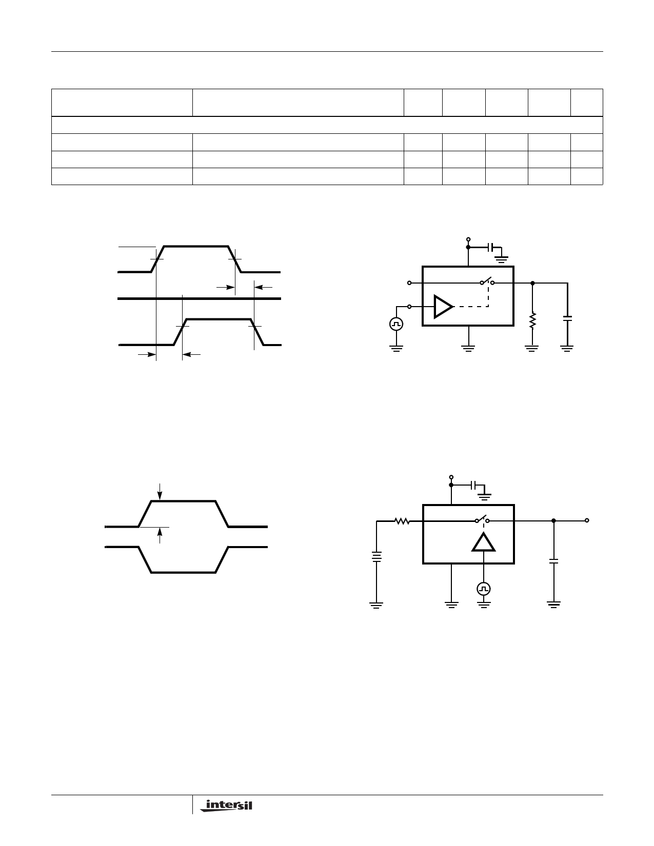
Test Circuits and Waveforms
LOGIC
INPUT
V+
0V
50%
tOFF
tr < 5ns
tf < 5ns
SWITCH
INPUT
VNO
SWITCH
OUTPUT 0V
VOUT
90%
tON
90%
Logic input waveform is inverted for switches that have the opposite
logic sense.
V+
C
SWITCH
INPUT
LOGIC
INPUT
NO or NC
IN
GND
COM
VOUT
RL CL
50Ω 35pF
Repeat test for all switches. CL includes fixture and stray
capacitance.
VOUT = V(NO or NC) -R----L-----+--R--R---L--(--O-----N----)
FIGURE 1A. MEASUREMENT POINTS
FIGURE 1. SWITCHING TIMES
FIGURE 1B. TEST CIRCUIT
V+
C
SWITCH
OUTPUT
VOUT
LOGIC
INPUT
ON
∆VOUT
OFF
Q = ∆VOUT x CL
V+
ON
0V
RG NO or NC
COM
VG
GND
IN
LOGIC
INPUT
FIGURE 2A. MEASUREMENT POINTS
FIGURE 2. CHARGE INJECTION
FIGURE 2B. TEST CIRCUIT
VOUT
CL
5 FN6094.3
November 5, 2004
5 Page 
ISL83699
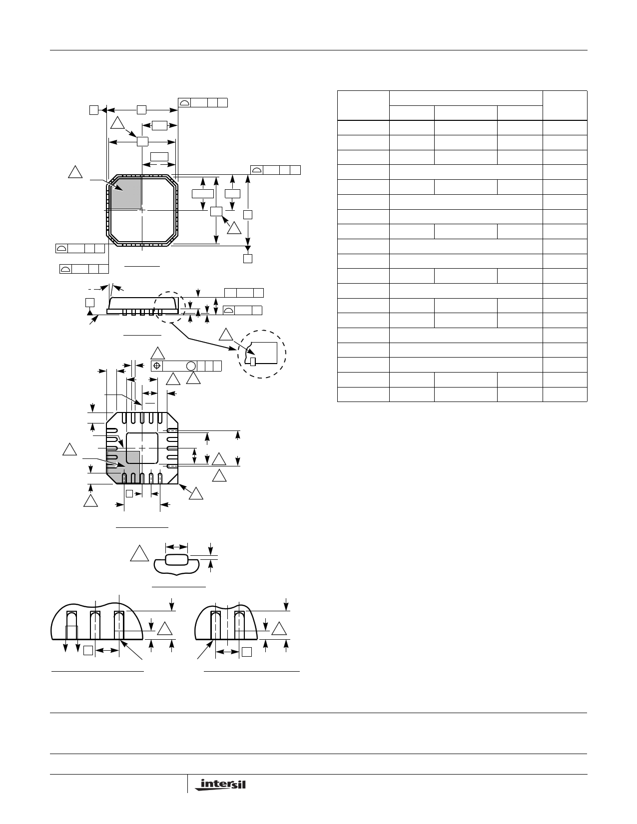
Quad Flat No-Lead Plastic Package (QFN)
Micro Lead Frame Plastic Package (MLFP)
2X
AD
0.15 C A
9 D/2
D1
6
INDEX
AREA
1
2
3
N
D1/2
2X
0.15 C B
E1/2 E/2
E1 E
2X
0.15 C B
2X
0.15 C A
TOP VIEW
9
B
4X
C
A2 A / / 0.10 C
0.08 C
SEATING PLANE SIDE VIEW
A3 A1
9
4X P
(DATUM B)
4X P
(DATUM A)
6
INDEX
AREA
NX L
8
NX b 5
0.10 M C A B
D2 7 8
D2
2N
NX k
Ne
(Nd-1)Xe
REF.
BOTTOM VIEW
NX b
5
1
2
3
(Ne-1)Xe
E2 REF.
7
E2/2
8
9
CORNER
OPTION 4X
A1
SECTION "C-C"
CL CL
L
L1 10
L
L1 10
e
CC
TERMINAL TIP
e
FOR ODD TERMINAL/SIDE
FOR EVEN TERMINAL/SIDE
L16.3x3
16 LEAD QUAD FLAT NO-LEAD PLASTIC PACKAGE
MILLIMETERS
SYMBOL
MIN
NOMINAL
MAX
NOTES
A 0.80 0.90 1.00 -
A1 -
- 0.05 -
A2 -
- 1.00 9
A3 0.20 REF 9
b 0.18 0.23 0.30 5, 8
D
3.00 BSC
-
D1 2.75 BSC 9
D2 1.35 1.50 1.65 7, 8, 10
E
3.00 BSC
-
E1 2.75 BSC 9
E2 1.35 1.50 1.65 7, 8, 10
e
0.50 BSC
-
k 0.20
-
--
L 0.30 0.40 0.50 8
N 16 2
Nd 4 3
Ne 4 3
P-
- 0.60 9
θ-
- 12 9
Rev. 1 6/04
NOTES:
1. Dimensioning and tolerancing conform to ASME Y14.5-1994.
2. N is the number of terminals.
3. Nd and Ne refer to the number of terminals on each D and E.
4. All dimensions are in millimeters. Angles are in degrees.
5. Dimension b applies to the metallized terminal and is measured
between 0.15mm and 0.30mm from the terminal tip.
6. The configuration of the pin #1 identifier is optional, but must be
located within the zone indicated. The pin #1 identifier may be
either a mold or mark feature.
7. Dimensions D2 and E2 are for the exposed pads which provide
improved electrical and thermal performance.
8. Nominal dimensions are provided to assist with PCB Land
Pattern Design efforts, see Intersil Technical Brief TB389.
9. Features and dimensions A2, A3, D1, E1, P & θ are present when
Anvil singulation method is used and not present for saw
singulation.
10. Compliant to JEDEC MO-220VEED-2 Issue C, except for the E2
and D2 MAX dimension.
All Intersil U.S. products are manufactured, assembled and tested utilizing ISO9000 quality systems.
Intersil Corporation’s quality certifications can be viewed at www.intersil.com/design/quality
Intersil products are sold by description only. Intersil Corporation reserves the right to make changes in circuit design, software and/or specifications at any time without
notice. Accordingly, the reader is cautioned to verify that data sheets are current before placing orders. Information furnished by Intersil is believed to be accurate and
reliable. However, no responsibility is assumed by Intersil or its subsidiaries for its use; nor for any infringements of patents or other rights of third parties which may result
from its use. No license is granted by implication or otherwise under any patent or patent rights of Intersil or its subsidiaries.
For information regarding Intersil Corporation and its products, see www.intersil.com
11 FN6094.3
November 5, 2004
11 Page | ||
| Páginas | Total 11 Páginas | |
| PDF Descargar | [ Datasheet FN6094.PDF ] | |
Hoja de datos destacado
| Número de pieza | Descripción | Fabricantes |
| FN6094 | Ultra Low ON-Resistance/ Low Voltage/ Single Supply/ Quad SPDT (Dual DPDT) Analog Switch | Intersil Corporation |
| FN6094 | Ultra Low ON-Resistance/ Low Voltage/ Single Supply/ Quad SPDT (Dual DPDT) Analog Switch | Intersil Corporation |
| Número de pieza | Descripción | Fabricantes |
| SLA6805M | High Voltage 3 phase Motor Driver IC. |
Sanken |
| SDC1742 | 12- and 14-Bit Hybrid Synchro / Resolver-to-Digital Converters. |
Analog Devices |
|
DataSheet.es es una pagina web que funciona como un repositorio de manuales o hoja de datos de muchos de los productos más populares, |
| DataSheet.es | 2020 | Privacy Policy | Contacto | Buscar |
