|
|
|
PDF FDG901 Data sheet ( Hoja de datos )
| Número de pieza | FDG901 | |
| Descripción | Slew Rate Control Driver IC for P-Channel MOSFETs | |
| Fabricantes | Fairchild Semiconductor | |
| Logotipo | ||
Hay una vista previa y un enlace de descarga de FDG901 (archivo pdf) en la parte inferior de esta página. Total 6 Páginas | ||
|
No Preview Available !
April 2002
FDG901D
Slew Rate Control Driver IC for P-Channel MOSFETs
General Description
The FDG901D is specifically designed to control the
turn on of a P-Channel MOSFET in order to limit the
inrush current in battery switching applications with high
capacitance loads. During turn-on the FDG901D drives
the MOSFET’s gate low with a regulated current
source, thereby controlling the MOSFET’s turn on. For
turn-off, the IC pulls the MOSFET gate up quickly, for
efficient turn off.
Applications
• Power management
• Battery Load switch
Features
• Three Programmable slew rates
• Reduces inrush current
• Minimizes EMI
• Normal turn-off speed
• Low-Power CMOS operates over wide voltage range
• Compact industry standard SC70-5 surface mount
package
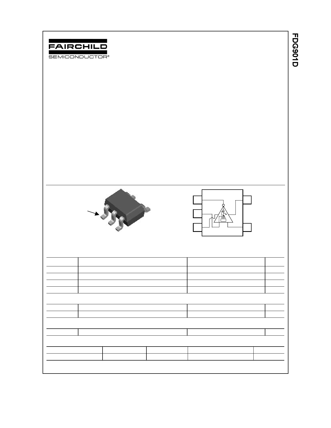
pin 1
GATE 1
SLEW 2
VDD 3
5 GND
4 LOGIC IN
Absolute Maximum Ratings TA=25oC unless otherwise noted
Symbol
Parameter
VDD
VIN
PD
TJ, TSTG
Supply Voltage
DC Input Voltage (Logic Inputs)
Power Dissipation for Single Operation @ 85°C
Operating and Storage Junction Temperature Range
Recommended Operating Range
VDD Supply Voltage
TJ Operating Temperature
Thermal Characteristics
RθJA Thermal Resistance, Junction-to-Ambient
(Note 1)
Package Marking and Ordering Information
Device Marking
Device
Reel Size
91
FDG901D
7’’
Ratings
-0.5 to 10
-0.7 to 6
150
-65 to +150
2.7 to 6.0
-40 to +125
425
Tape width
8mm
Units
V
V
mW
°C
V
°C
°C/W
Quantity
3000 units
2002 Fairchild Semiconductor Corporation
FDG901D rev. E (W)
1 page 
The Slew Rate Control Driver (FDG901D) is designed to give a programmed choice of one of
three steady dv/dt states on the output during turn-on. To change the dv/dt value, the user needs
to use the Slew Rate Control Pin (Pin 2). To utilize the smallest current setting (≈10 nA) from the
IC, a voltage equal to Vdd must be applied to the Slew Rate Control Pin 2. To use the next
higher current setting (≈1 µA) a voltage equal to Ground must be applied to Pin 2. To achieve the
highest current setting (≈ 80 µA) or obtain a faster switching speed, the Slew Rate Pin2 must be
open (floating). A higher value of capacitance will result in a slower switching rate. To determine
the switching times of each setting use the simple equation:
t
=
Qg
IG
where Qg is the Gate charge in nC for a given MOSFET and IG is the gate current controlled by
the slew rate pin.
Below is a captured image from an oscilloscope depicting the device response. The FDG901D
was connected to control an FDG258P P-Channel DMOS. The Slew Rate control pin was set to
open (floating state).
Test Conditions:
VDD = 5.5V
VIN = 5.5V
RLOAD = 1.5Ω
VIN
Vgate (inverted)
VRLoad
Circuit waveforms for an FDG901D controlling a P-Channel FDG258P MOSFET.
FDG901D rev. D (W)
5 Page | ||
| Páginas | Total 6 Páginas | |
| PDF Descargar | [ Datasheet FDG901.PDF ] | |
Hoja de datos destacado
| Número de pieza | Descripción | Fabricantes |
| FDG901 | Slew Rate Control Driver IC for P-Channel MOSFETs | Fairchild Semiconductor |
| FDG901D | Slew Rate Control Driver IC for P-Channel MOSFETs | Fairchild Semiconductor |
| Número de pieza | Descripción | Fabricantes |
| SLA6805M | High Voltage 3 phase Motor Driver IC. |
Sanken |
| SDC1742 | 12- and 14-Bit Hybrid Synchro / Resolver-to-Digital Converters. |
Analog Devices |
|
DataSheet.es es una pagina web que funciona como un repositorio de manuales o hoja de datos de muchos de los productos más populares, |
| DataSheet.es | 2020 | Privacy Policy | Contacto | Buscar |