|
|
|
PDF LZ93N61 Data sheet ( Hoja de datos )
| Número de pieza | LZ93N61 | |
| Descripción | Timing Pulse Generator LSI for CCD | |
| Fabricantes | Sharp Electrionic Components | |
| Logotipo | ||
Hay una vista previa y un enlace de descarga de LZ93N61 (archivo pdf) en la parte inferior de esta página. Total 12 Páginas | ||
|
No Preview Available !
LZ93N61
LZ93N61
DESCRIPTION
The LZ93N61 is a CMOS timing generator LSI
which provides timing pulses used to drive a
CCD area sensor, in combination with the SSG
LSI (LZ93NI 9, LZ93B53).
FEATURES
q Switchable between 270000 pixels CCD and
320000 pixels CCD
q Switchable between NTSC (EIA) and PAL
(CCIR) systems
q Internal electronic shutter :
Shutter speed is selectable from 1/W, 1/125,
1/250, 1/500, 1/1 000, 1/2 000, 1/4 000 and
1/10 000 s, in addition to this, 1/100 s (PAL
: 1/120 s) in Flicker-less mode using parallel
or serial code. Shutter speed can also be
controlled in 1 H period using an external
trigger to the EXST input.
c Single +5 V power supply
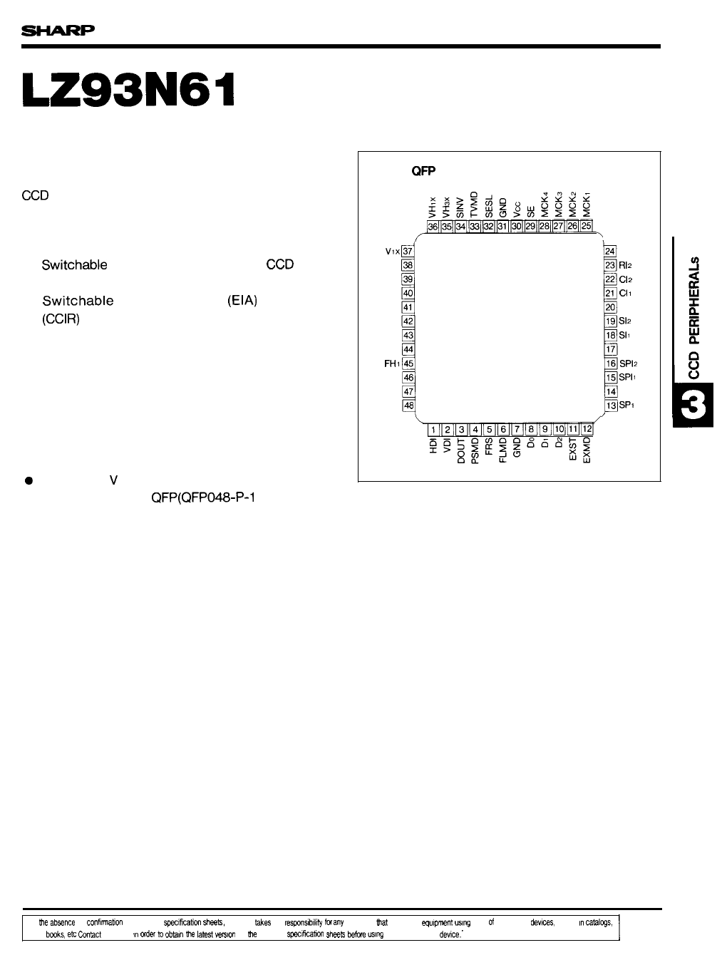
q Package : 48-pin QFP(QFP048-P-I 01 O)
Timing Pulse Generator LSI for CCD
PIN CONNECTIONS
48-PIN QFP
TOP VIEW
IVlx 37
V2X 3a
V3X 39
V4X 40
OFDX 41
FR 42
GND 43
FH2 44
FHI 45
CKI 46
CKO 47
TSTI W
o
124R12
23 R12
22 C12
21 CI1
20 FCDS
19 S12
18 SI1
17 FS
16 SP12
15 SPII
14 SP2
13 SPI
“In tie abeence of conf[mtlon by device acecification ehwf?, WARP fakee no reswns!blhty b anY defects hat recur In qutpment USIW any of WARPS davIces, show In Cahlws,
287deta bwks, etc hn~ct WARP !n mder to obtain tie Iateat vefilon of he device swIkaiim shw~ ktie USIW any 8HARPs dewce.”
I
1 page 
U93N61
PU.or-N. 1 C--V-M--R--~-
15 SPI 1
16 SP12
17 FS
18 SI 1
19 S12
20 FCDS
21 c11
22 C12
23 RI j
24 R12
25 MCKI
26 MCK2
27 MCK3
28 MCK4
29 SE
30 Vcc
31 GND
II/n
-$-
I M.-LA—R....~.
PIN NAME
IC
SPI and SP2 phase
m control input 1
FUNCTON
The SPII pin sets the falling edge of COICS sampling
pulses SP1 (pin 13) and SP2 (pin 14).
Ic
SP1 and SPZ phase The SP12 pin sets the rising edge of color sampling
N control input 2
pulses SPI (pin 13) and SP2 (pin 14).
o n CDS pulse 2
The FS pin outputs the pulses for sampling output
signals of CCD.
Ic m FS phase control input 1 The SII pin sets the phase of the FS (pin 17).
Ic nn FS phase control input 2 The SIZ pin sets the width of the FS (pin 17).
o n FCDS pulse 1
The FCDS pin outputs the pulse to clamp the out-
put signals of CCD.
Ic
FCDS phase control
m input 1
The Cl 1 pin sets the phase of the FCDS (pin 20).
FCDS phase control
Ic N input 2
The CIZ pin sets the width of the FCDS (pin 20).
FR phase control
Ic nn input 1
The RI I pin sets the pahse of the FR (pin 42).
Ic
FR phase control
nn input 2
The R12 pin sets the width of the FR (pin 42).
o nn Clock output 1
The MCKI pin outputs 1/2 dividing pulse of CKI (pin
46). It is the same phase with the FH i (pin 45).
o nn Clink output 2
The MCK2 pin outputs 1/2 dividi~ pulse of CKI (pin
46). It is delayad by approximately 90° in phase with
respect to FH1 (pin 45).
o nrl Clwk output 3
Tk MCK3 pin outputs 1/2 dividing pulse of CKI (pin
46). It is the same phase with the FHz (pin 44).
o m Clock output 4
The MCK4 pin outputs 1/2 dividing pulse of CKI (pin
46). It is delayed by approximately 90” in phase witi
respect to FH2 (pin 44).
The SE pin outputs the demodulation carrier of out-
put signals of CCD, and input the switching signal
Color demodulation
of color sampling pulses SP1 (pin 13) and SPZ (pin
o rL pulw
14). It outputs 1/4 dividing pulse of the CKI input
(pin 46), and selects the phase in mmbination with
the SESL (pin 32) and the SINV (pin 34).
– — Power supply
The Vcc is a + 5 V power supply pin.
– – Ground
The GND is a ground pin.
291
5 Page 
LZ93N61
(ODD FIELD)
HD
VI x
V2X
V3X
v..
VHIX
VH3X
OFDX
(EVEN FIELD)
HD
v!.
V2X
V3X
V4X
VHIX
VH3X
OFDX
CHARGE READ TIMING < NTSC >
18 H
19 H
121 2(01
}~.r+.
-,5~98~——1! .—~5~wI
78 118 3;2;
898
78
120
118
I —I ——II ?z,?”~
28Il H
281 H
121 2(o)
=..———~
120
I
6a
—,
I
1
L-—
28
128
+~
(Ist, 3rd FIELD)
CHARGE READ TIMING < PAL >
HD
VIX
V2X
V3X
V4X
V HI X
VH3X
OFDX
(2nd, 4th FIELD)
HD
VI x
V2X
V3X
V4X
VHIX
VH3X
OFDX
,4
— ———-8112 7M
332 H
o
120
_—— —
333 H
12WOI
lm
~ _—— —
?~118
II
32—2 ———
1
118
I
—~—Y___ ~
——m
I
i 2_8 _— .——,
IL
128
I
——wY—
11 Page | ||
| Páginas | Total 12 Páginas | |
| PDF Descargar | [ Datasheet LZ93N61.PDF ] | |
Hoja de datos destacado
| Número de pieza | Descripción | Fabricantes |
| LZ93N61 | Timing Pulse Generator LSI for CCD | Sharp Electrionic Components |
| Número de pieza | Descripción | Fabricantes |
| SLA6805M | High Voltage 3 phase Motor Driver IC. |
Sanken |
| SDC1742 | 12- and 14-Bit Hybrid Synchro / Resolver-to-Digital Converters. |
Analog Devices |
|
DataSheet.es es una pagina web que funciona como un repositorio de manuales o hoja de datos de muchos de los productos más populares, |
| DataSheet.es | 2020 | Privacy Policy | Contacto | Buscar |