|
|
|
PDF 95144 Data sheet ( Hoja de datos )
| Número de pieza | 95144 | |
| Descripción | XC95144 In-System Programmable CPLD | |
| Fabricantes | Xilinx Inc | |
| Logotipo | ||
Hay una vista previa y un enlace de descarga de 95144 (archivo pdf) en la parte inferior de esta página. Total 12 Páginas | ||
|
No Preview Available !
93LCS56/66
2K/4K 2.5V Microwire® Serial EEPROM with Software Write Protect
FEATURES
• Single supply with programming operation down
to 2.5V
• Low power CMOS technology
- 1 mA active current typical
- 5 µA standby current (typical) at 3.0V
• x16 memory organization
- 128x16 (93LCS56)
- 256x16 (93LCS66)
• Software write protection of user defined memory
space
• Self timed erase and write cycles
• Automatic ERAL before WRAL
• Power on/off data protection
• Industry standard 3-wire serial I/O
• Device status signal during E/W
• Sequential READ function
• 1,000,000 E/W cycles guaranteed
• Data retention > 200 years
• 8-pin PDIP/SOIC and 14-pin SOIC packages
• Temperature ranges supported
- Commercial (C):
- Industrial (I):
0˚C to +70˚C
-40˚C to +85˚C
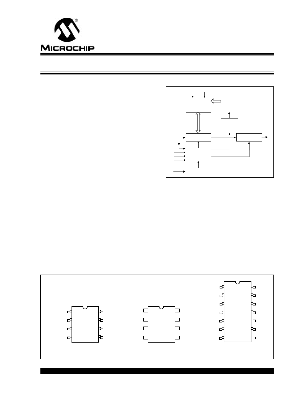
BLOCK DIAGRAM
VCC
V SS
MEMORY
ARRAY
ADDRESS
DECODER
DI
PRE
PE
CS
DATA REGISTER
MODE
DECODE
LOGIC
ADDRESS
COUNTER
OUTPUT
BUFFER
DO
CLOCK
CLK GENERATOR
DESCRIPTION
The Microchip Technology Inc. 93LCS56/66 are low volt-
age Serial Electrically Erasable PROMs with memory
capacities of 2K bits/4K bits respectively. A write protect
register is included in order to provide a user defined
region of write protected memory. All memory locations
greater than or equal to the address placed in the write
protect register will be protected from any attempted write
or erase operation. It is also possible to protect the
address in the write protect register permanently by using
a one time only instruction (PRDS). Any attempt to alter
data in a register whose address is equal to or greater
than the address stored in the protect register will be
aborted. Advanced CMOS technology makes this device
ideal for low power non-volatile memory applications.
PACKAGE TYPES
CS
CLK
DI
DO
DIP
18
27
36
45
93LCS56
93LCS66
VCC
PRE
PE
VSS
CS
CLK
DI
DO
SOIC
18
27
36
45
93LCS56
93LCS66
VCC
PRE
PE
VSS
SOIC
NC 1
CS 2
CLK 3
NC 4
DI 5
DO 6
NC 7
14 NC
13 VCC
12 PRE
11 NC
10 PE
9 VSS
8 NC
93LCS56
93LCS66
Microwire is a registered trademark of National Semiconductor Incorporated.
© 1996 Microchip Technology Inc.
Preliminary
DS11181D-page 1
This document was created with FrameMaker 4 0 4
1 page 
The DO pin indicates the READY/BUSY status of the
device if CS is brought high after a minimum of 250 ns
(TCSL) and before the entire write cycle is complete. DO
at logical “0” indicates that programming is still in
progress. DO at logical “1” indicates that the register at
the specified address has been written with the data
specified and the device is ready for another instruc-
tion. WRITE instruction is valid only if specified address
is unprotected.
The WRITE cycle takes 4 ms per word typical.
2.8 Erase All (ERAL)
The ERAL instruction will erase the entire memory
array to the logical “1”. The ERAL cycle is identical to
the ERASE cycle except for the different opcode. The
ERAL cycle is completely self-timed and commences at
the falling edge of the CS. PE pin MUST be held “high”
while loading the instruction but becomes “don't care”
thereafter. Clocking of the CLK pin is not necessary
after the device has entered the self clocking mode.
The ERAL instruction is guaranteed at VCC = 4.5 to 6V
and valid only when Protect Register is cleared.
The DO pin indicates the READY/BUSY status of the
device if CS is brought high after a minimum of 250 ns
low (TCSL) and before the entire write cycle is complete.
The ERAL cycle takes 15 ms maximum (8 ms typical).
2.9 Write All (WRAL)
The WRAL instruction will write the entire memory array
with the data specified in the command. The WRAL
cycle is completely self-timed and commences at the
falling edge of the CS. PE pin MUST be held “high”
while loading the instruction but becomes “don't care”
thereafter. Clocking of the CLK pin is not necessary
after the device has entered the self clocking mode.
The WRAL command does include an automatic ERAL
cycle for the device. Therefore, the WRAL instruction
does not require an ERAL instruction but the chip must
be in the EWEN status. The WRAL instruction is guar-
anteed at VCC = 4.5 to 6V and valid only when Protect
Register is cleared.
The DO pin indicates the READY/BUSY status of the
device if CS is brought high after a minimum of 250 ns
low (TCSL).
The WRAL cycle takes 30 ms maximum (16 ms typical).
Note:
In order to execute either READ, EWEN,
ERAL, WRITE, WRAL, or EWDS instruc-
tions, the Protect Register Enable (PRE)
pin must be held LOW.
93LCS56/66
2.10 Protect Register Read (PRREAD)
The Protect Register Read (PRREAD) instruction out-
puts the address stored in the Protect Register on the
DO pin. The PRE pin MUST be held HIGH when load-
ing the instruction and remains HIGH until CS goes
LOW. A dummy zero bit precedes the 8-bit output
string. The output data bits in the memory Protect Reg-
ister will toggle on the rising edge of the CLK as in the
READ mode.
2.11 Protect Register Enable (PREN)
The Protect Register Enable (PREN) instruction is used
to enable the PRCLEAR, PRWRITE, and PRDS
modes. Before the PREN mode can be entered, the
device must be in the EWEN mode. Both PRE and PE
pins MUST be held “high” while loading the instruction.
The PREN instruction MUST immediately precede a
PRCLEAR, PRWRITE, or PRDS instruction.
2.12 Protect Register Clear (PRCLEAR)
The Protect Register Clear (PRCLEAR) instruction
clears the address stored in the Protect Register and,
therefore, enables all registers for programming
instructions such as ERASE, ERAL, WRITE, and
WRAL. The PRE and PE pin MUST be held HIGH when
loading the instruction. Thereafter, PRE and PE pins
become “don't care”. A PREN instruction must immedi-
ately precede a PRCLEAR instruction.
2.13 Protect Register Write (PRWRITE)
The Protect Register Write (PRWRITE) instruction
writes into the Protect Register the address of the first
register to be protected. After this instruction is exe-
cuted, all registers whose memory addresses are
greater than or equal to the address pointer specified in
the Protect register are protected from any program-
ming instructions. Note that a PREN instruction must
be executed before a PRWRITE instruction and, the
Protect Register must be cleared (by a PRCLEAR
instruction) before executing the PRWRITE instruction.
The PRE and PE pins MUST be held HIGH while load-
ing PRWRITE instruction. After the instruction is
loaded, they become “don't care”.
2.14 Protect Register Disable (PRDS)
The Protect Register Disable (PRDS) instruction is a
ONE TIME ONLY instruction to permanently set the
address specified in the Protect Register. Any attempts
to change the address pointer will be aborted. The PRE
and PE pins MUST be held HIGH while loading PRDS
instruction. After the instruction is loaded, they become
“don't care”. Note that a PREN instruction must be exe-
cuted before a PRDS instruction.
© 1996 Microchip Technology Inc.
Preliminary
DS11181D-page 5
5 Page 
93LCS56/66
93LCS56/66 Product Identification System
To order or to obtain information, e.g., on pricing or delivery, please use the listed part numbers, and refer to the factory or the listed
sales offices.
93LCS56/66 –
/P
Package:
P = Plastic DIP (300 mil Body), 8-lead
SN = Plastic SOIC (150 mil Body), 8-lead
SM = Plastic SOIC (207 mil Body), 8-lead
SL = Plastic SOIC (150 mil Body), 14-lead
Temperature
Range:
Blank = 0°C to +70°C
I = -40°C to +85°C
Device:
93LCS56/66 Microwire Serial EEPROM
93LCS56T/66T Microwire Serial EEPROM (Tape and Reel)
© 1996 Microchip Technology Inc.
Preliminary
DS11181D-page 11
11 Page | ||
| Páginas | Total 12 Páginas | |
| PDF Descargar | [ Datasheet 95144.PDF ] | |
Hoja de datos destacado
| Número de pieza | Descripción | Fabricantes |
| 95144 | XC95144 In-System Programmable CPLD | Xilinx Inc |
| Número de pieza | Descripción | Fabricantes |
| SLA6805M | High Voltage 3 phase Motor Driver IC. |
Sanken |
| SDC1742 | 12- and 14-Bit Hybrid Synchro / Resolver-to-Digital Converters. |
Analog Devices |
|
DataSheet.es es una pagina web que funciona como un repositorio de manuales o hoja de datos de muchos de los productos más populares, |
| DataSheet.es | 2020 | Privacy Policy | Contacto | Buscar |