|
|
|
PDF AD2S82A Data sheet ( Hoja de datos )
| Número de pieza | AD2S82A | |
| Descripción | Variable Resolution/ Monolithic Resolver-to-Digital Converters | |
| Fabricantes | Analog Devices | |
| Logotipo | ||
Hay una vista previa y un enlace de descarga de AD2S82A (archivo pdf) en la parte inferior de esta página. Total 16 Páginas | ||
|
No Preview Available !
a
Variable Resolution, Monolithic
Resolver-to-Digital Converters
AD2S81A/AD2S82A
FEATURES
Monolithic (BiMOS ll) Tracking R/D Converter
Ratiometric Conversion
Low Power Consumption: 300 mW Typ
Dynamic Performance Set by User
Velocity Output
ESD Class 2 Protection (2,000 V Min)
AD2S81A
28-Lead DIP Package
Low Cost
AD2S82A
44-Lead PLCC Package
10-, 12-, 14- and 16-Bit Resolution Set by User
High Max Tracking Rate 1040 RPS (10 Bits)
VCO Output (Inter LSB Output)
Data Complement Facility
Industrial Temperature Range
APPLICATIONS
DC Brushless and AC Motor Control
Process Control
Numerical Control of Machine Tools
Robotics
Axis Control
GENERAL DESCRIPTION
The AD2S82A is a monolithic 10-, 12-, 14- or 16-bit tracking
resolver-to-digital converter contained in a 44-lead J leaded
PLCC package. Two extra functions are provided in the new
surface mount package–COMPLEMENT and VCO output.
The AD2S81A is a monolithic 12-bit fixed resolution tracking
resolver-to-digital converter packaged in a 28-lead DIP.
The converters allow users to select their own dynamic performance
with external components. This allows the users great flexibility in
defining the converter that best suits their system requirements.
The AD2S82A allows users to select the resolution to be 10, 12,
14 or 16 bits and to track resolver signals rotating at up to 1040
revs per second (62,400 rpm) when set to 10-bit resolution.
The AD2S81A and AD2S82A convert resolver format input
signals into a parallel natural binary digital word using a ratio-
metric tracking conversion method. This ensures high-noise
immunity and tolerance of lead length when the converter is
remote from the resolver.
The output word is in a three-state digital logic form available in
two bytes on the 16 output data lines for the AD2S82A and on
eight output data lines for the AD2S81A. BYTE SELECT,
ENABLE and INHIBIT pins ensure easy data transfer to 8- and
16-bit data buses, and outputs are provided to allow for cycle or
pitch counting in external counters.
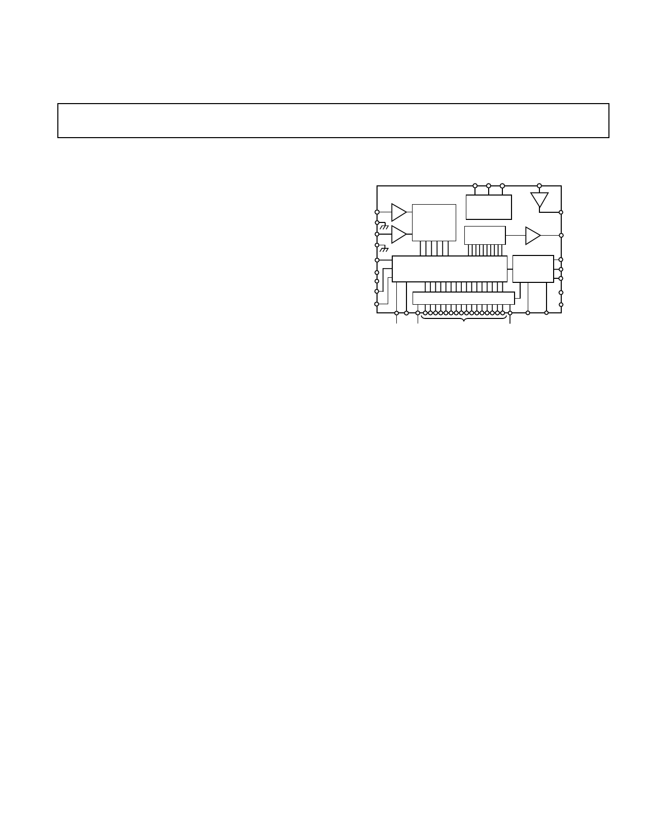
AD2S82A FUNCTIONAL BLOCK DIAGRAM
SIN I/P
SIGNAL
GND
COS I/P
ANALOG
GND
RIPPLE
CLK
+12V
–12V
COMP
DATA
LOAD
DEMOD DEMOD INTEGRATOR
I/P O/P
I/P
AD2S82A
A1
SEGMENT
SWITCHING
A2
PHASE
SENSITIVE
DETECTOR
R-2R
DAC
A3
INTEGRATOR
O/P
AC ERROR
O/P
16-BIT
UP/DOWN COUNTER
VCO DATA
TRANSFER
LOGIC
OUTPUT DATA LATCH
SC2
SC1 ENABLE
16 DATA BITS
BUSY DIR
BYTE
SELECT
VCO I/P
INHIBIT
VCO O/P
+5V
DIGITAL
GND
An analog signal proportional to velocity is also available and
can be used to replace a tachogenerator.
PRODUCT HIGHLIGHTS
Monolithic. A one-chip solution reduces the package size re-
quired and increases the reliability.
Resolution Set by User. Two control pins are used to select
the resolution of the AD2S82A to be 10, 12, 14 or 16 bits al-
lowing the user to use the AD2S82A with the optimum resolu-
tion for each application.
Ratiometric Tracking Conversion. Conversion technique
provides continuous output position data without conversion
delay and is insensitive to absolute signal levels. It also provides
good noise immunity and tolerance to harmonic distortion on
the reference and input signals.
Dynamic Performance Set by the User. By selecting exter-
nal resistor and capacitor values the user can determine band-
width, maximum tracking rate and velocity scaling of the
converter to match the system requirements. The external com-
ponents required are all low cost, preferred value resistors and
capacitors, and the component values are easy to select using
the simple instructions given.
Velocity Output. An analog signal proportional to velocity is
available and is linear to typically one percent. This can be used
in place of a velocity transducer in many applications to provide
loop stabilization in servo controls and velocity feedback data.
Low Power Consumption. Typically only 300 mW.
MODELS AVAILABLE
Information on the models available is given in the Ordering
Guide.
REV. B
Information furnished by Analog Devices is believed to be accurate and
reliable. However, no responsibility is assumed by Analog Devices for its
use, nor for any infringements of patents or other rights of third parties
which may result from its use. No license is granted by implication or
otherwise under any patent or patent rights of Analog Devices.
One Technology Way, P.O. Box 9106, Norwood, MA 02062-9106, U.S.A.
Tel: 781/329-4700 World Wide Web Site: http://www.analog.com
Fax: 781/326-8703
© Analog Devices, Inc., 1998
1 page 
AD2S81A/AD2S82A
RECOMMENDED OPERATING CONDITIONS
Power Supply Voltage (+VS to –VS) . . . . . . . . . ± 12 V dc ± 10%
Power Supply Voltage VL . . . . . . . . . . . . . . . . . . +5 V dc ± 10%
Analog Input Voltage (SIN and COS) . . . . . . . . 2 V rms ± 10%
Analog Input Voltage (REF) . . . . . . . . . . . . . . 1 V to 8 V peak
Signal and Reference Harmonic Distortion . . . . . . . 10% (max)
Phase Shift Between Signal and Reference . ± 10 Degrees (max)
Ambient Operating Temperature Range
Commercial (JD) . . . . . . . . . . . . . . . . . . . . . . 0°C to +70°C
Industrial (HP, JP, KP, LP) . . . . . . . . . . . . –40°C to +85°C
PIN FUNCTION DESCRIPTIONS
Mnemonic
Description
REFERENCE I/P Reference Signal Input
DEMOD I/P
Demodulator Input
AC ERROR O/P Ratio Multiplier Output
COS I/P
Cosine Input
ANALOG GND Power Ground
SIGNAL GND
Resolver Signal Ground
SIN I/P
Sine Input
+VS
DB1–DB16
Positive Power Supply
Parallel Output Data
+VL
ENABLE
Logic Power Supply
Logic Hi-Output Data in High Impedance
State Logic Lo Present Data to the Output Latches
BYTE SELECT Logic Hi-Most Significant Byte to DB1–DB8
INHIBIT
Logic Lo-Most Significant Byte to DB1–DB8
Logic Lo Inhibits Data Transfer to Output Latches
DIGITAL GND Digital Ground
SC1–SC2*
Select Converter Resolution
DATA LOAD*
Logic Lo DB1–DB16 Inputs
Logic Hi DB1–DB16 Outputs
BUSY
Converter Busy, Data Not Valid While Busy Hi
DIR Logic State Defines Direction of Input Signal Rotation
RIPPLE CLK
Positive Pulse when Converter Output Changes from
1s to All 0s or Vice Versa
–VS
VCO I/P
Negative Power Supply
VCO Input
INTEGRATOR I/P Integrator Input
INTEGRATOR O/P Integrator Output
DEMOD O/P
Demodulator Output
COMPLEMENT* Active Logic Lo
VCO O/P*
VCO Output
*AD2S82A Only.
Bit Weight Table
Binary
Bits (N)
Resolution Degrees
(2N) /Bit
Minutes
/Bit
Seconds
/Bit
0
1 360.0
21600.0
1296000.0
1
2 180.0
10800.0
648000.0
2
4 90.0
5400.0
324000.0
3
8 45.0
2700.0
162000.0
4
16 22.5
1350.0
81000.0
5
32 11.25
675.0
40500.0
6
64 5.625
337.5
20250.0
7
128
2.8125
168.75
10125.0
8
256
1.40625
84.375
5062.5
9
512
0.703125
42.1875
2531.25
10
1024
0.3515625 21.09375
1265.625
11
2048
0.1757813 10.546875
632.8125
12
4096
0.0878906
5.273438
316.40625
13
8192
0.0439453
2.636719
158.20313
14
116384
0.0219727
1.318359
79.10156
15
32768
0.0109836
0.659180
39.55078
16
65536
0.0054932
0.329590
19.77539
17
131072
0.0027466
0.164795
9.88770
18
262144
0.0013733
0.082397
4.94385
ABSOLUTE MAXIMUM RATINGS1 (with respect to GND)
+VS2 . . . . . . . . . . . . . . . . . . . . . . . . . . . . . . . . . . . . . +14 V dc
–VS . . . . . . . . . . . . . . . . . . . . . . . . . . . . . . . . . . . . . . –14 V dc
+VL . . . . . . . . . . . . . . . . . . . . . . . . . . . . . . . . . . . . . . . . . . +VS
Reference . . . . . . . . . . . . . . . . . . . . . . . . . . . . . . . +14 V to –VS
SIN . . . . . . . . . . . . . . . . . . . . . . . . . . . . . . . . . . . +14 V to –VS
COS . . . . . . . . . . . . . . . . . . . . . . . . . . . . . . . . . . +14 V to –VS
Any Logical Input . . . . . . . . . . . . . . . . . . . –0.4 V dc to +VL dc
Demodulator Input . . . . . . . . . . . . . . . . . . . . . . . +14 V to –VS
Integrator Input . . . . . . . . . . . . . . . . . . . . . . . . . . +14 V to –VS
VCO Input . . . . . . . . . . . . . . . . . . . . . . . . . . . . . +14 V to –VS
Power Dissipation . . . . . . . . . . . . . . . . . . . . . . . . . . . . 860 mW
Operating Temperature
Commercial (JD) . . . . . . . . . . . . . . . . . . . . . . 0°C to +70°C
Industrial (HP, JP, KP, LP) . . . . . . . . . . . . . –40°C to +85°C
Storage Temperature (All Grades) . . . . . . . . . –65°C to +150°C
Lead Temperature (Soldering, 10 sec) . . . . . . . . . . . . +300°C
CAUTION
1. Absolute Maximum Ratings are those values beyond which damage to the
device may occur.
2. Correct polarity voltages must be maintained on the +V S and –VS pins.
AD2S81A/AD2S82A PIN CONFIGURATIONS
REFERENCE I/P 1
28 DEMOD O/P
DEMOD I/P 2
27 INTEGRATOR O/P
AC ERROR O/P 3
26 INTEGRATOR I/P
COS I/P 4
25 VCO I/P
ANALOG GND
SIN I/P
+VS
MSB DB1
5 24 –VS
6 AD2S81A 23 RIPPLE CLK
7 TOP VIEW 22 DIR
8 (Not to Scale) 21 BUSY
DB2 9
20 DIGITAL GND
DB3 10
19 INHIBIT
DB4 11
18 BYTE SELECT
DB5 12
17 ENABLE
DB6 13
DB7 14
16 +VL
15 DB8 LSB
SIN O/P 7
+VS 8
NC 9
MSB DB1 10
DB2 11
DB3 12
DB4 13
DB5 14
DB6 15
DB7 16
DB8 17
6 5 4 3 2 1 44 43 42 41 40
PIN 1
IDENTIFIER
AD2S82A
TOP VIEW
(Not to Scale)
39 –VS
38 RIPPLE CLK
37 DIR
36 BUSY
35 DATA LOAD
34 COMPLEMENT
33 SC2
32 SC1
31 DIGITAL GND
30 INHIBIT
29 NC
18 19 20 21 22 23 24 25 26 27 28
NC = NO CONNECT
REV. B
–5–
5 Page 
AD2S81A/AD2S82A
Ratio Multiplier
The ratio multiplier is the input section of the AD2S81A/
AD2S82A and compares the signal from the resolver input
angle, θ, to the digital angle, φ, held in the counter. Any differ-
ence between these two angles results in an analog voltage at
the AC ERROR OUTPUT. This circuit function has histori-
cally been called a “Control Transformer” as it was originally
performed by an electromechanical device known by that name.
The AC ERROR signal is given by
A1 sin (θ – φ) sin ωt
where ω = 2 π fREF
fREF = reference frequency
A1, the gain of the ratio multiplier stage is 14.5.
So for 2 V rms inputs signals
AC ERROR output in volts/(bit of error)
=
2
×
sin
360
n
×
A1
Where n = bits per rev
= 1,024 for 10-bits resolution
= 4,096 for 12 bits
= 16,384 for 14 bits
= 65,536 for 16 bits
Giving an AC ERROR O/P
= 178 mV/bit @ 10-bits resolution
= 44.5 mV/bit @ 12 bits
= 11.125 mV/bit @ 14 bits
= 2.78 mV/bit @ 16 bits
The ratio multiplier will work in exactly the same way whether
the AD2S81A/AD2S82A is connected as a tracking converter or
as a control transformer, where data is preset into the counters
using the DATA LOAD pin.
HF Filter
The AC ERROR OUTPUT may be fed to the PSD via a simple
ac coupling network (R2, C1) to remove any dc offset at this
point. Note, however, that the PSD of the AD2S81A/AD2S82A
is a wideband demodulator and is capable of aliasing HF noise
down to within the loop bandwidth. This is most likely to hap-
pen where the resolver is situated in particularly noisy environ-
ments, and the user is advised to fit a simple HF filter R1, C2
prior to the phase sensitive demodulator.
The attenuation and frequency response of a filter will affect the
loop gain and must be taken into account in deriving the loop
transfer function. The suggested filter (R1, C1, R2, C2) is shown
in Figure 1 and gives an attenuation at the reference frequency
(fREF) of 3 times at the input to the phase sensitive demodulator.
Values of components used in the filter must be chosen to en-
sure that the phase shift at fREF is within the allowable signal to
reference phase shift of the converter.
Phase Sensitive Demodulator
The phase sensitive demodulator is effectively ideal and devel-
ops a mean dc output at the DEMODULATOR O/P pin of
±2
π
2
× (DEMODULATOR I/P
rms voltage)
for sinusoidal signals in phase or antiphase with the reference
(for a square wave the DEMODULATOR O/P voltage will
equal the DEMODULATOR I/P). This provides a signal at the
DEMODULATOR O/P which is a dc level proportional to the
positional error of the converter.
DC Error Scaling = 160 mV/bit (10-bits resolution)
= 40 mV/bit (12-bits resolution)
= 10 mV/bit (14-bits resolution)
= 2.5 mV/bit (16-bits resolution)
When the tracking loop is closed, this error is nulled to zero
unless the converter input angle is accelerating.
Integrator
The integrator components (R4, C4, R5, C5) are external to
the AD2S81A/AD2S82A to allow the user to determine the
optimum dynamic characteristics for any given application. The
Component Selection section explains how to select compo-
nents for a chosen bandwidth.
Since the output from the integrator is fed to the VCO INPUT,
it is proportional to velocity (rate of change of output angle)
and can be scaled by selection of R6, the VCO input resistor.
This is explained in the Voltage Controlled Oscillator (VCO)
section below.
To prevent the converter from “flickering” (i.e., continually
toggling by ±1 bit when the quantized digital angle, φ, is not an
exact representation of the input angle, θ), feedback is internally
applied from the VCO to the integrator input to ensure that the
VCO will only update the counter when the error is greater than
or equal to 1 LSB. In order to ensure that this feedback “hyster-
esis” is set to 1 LSB the input current to the integrator must be
scaled to be 100 nA/bit. Therefore,
R4 = DC Error Scaling (mV /bit )
100 (nA /bit )
Any offset at the input of the integrator will affect the accuracy
of the conversion as it will be treated as an error signal and
offset the digital output. One LSB of extra error will be
added for each 100 nA of input bias current. The method of
adjusting out this offset is given in the Component Selection
section.
Voltage Controlled Oscillator (VCO)
The VCO is essentially a simple integrator feeding a pair of dc
level comparators. Whenever the integrator output reaches one
of the comparator threshold voltages, a fixed charge is injected
into the integrator input to balance the input current. At the
same time the counter is clocking either up or down, dependent
on the polarity of the input current. In this way the counter is
clocked at a rate proportional to the magnitude of the input
current of the VCO.
REV. B
–11–
11 Page | ||
| Páginas | Total 16 Páginas | |
| PDF Descargar | [ Datasheet AD2S82A.PDF ] | |
Hoja de datos destacado
| Número de pieza | Descripción | Fabricantes |
| AD2S82A | Variable Resolution/ Monolithic Resolver-to-Digital Converters | Analog Devices |
| Número de pieza | Descripción | Fabricantes |
| SLA6805M | High Voltage 3 phase Motor Driver IC. |
Sanken |
| SDC1742 | 12- and 14-Bit Hybrid Synchro / Resolver-to-Digital Converters. |
Analog Devices |
|
DataSheet.es es una pagina web que funciona como un repositorio de manuales o hoja de datos de muchos de los productos más populares, |
| DataSheet.es | 2020 | Privacy Policy | Contacto | Buscar |