|
|
|
PDF AD5242 Data sheet ( Hoja de datos )
| Número de pieza | AD5242 | |
| Descripción | 2-Channel/ 256-Position Digital Potentiometer | |
| Fabricantes | Analog Devices | |
| Logotipo | ||
Hay una vista previa y un enlace de descarga de AD5242 (archivo pdf) en la parte inferior de esta página. Total 20 Páginas | ||
|
No Preview Available !
I2C-Compatible,
256-Position Digital Potentiometers
AD5241/AD5242
FEATURES
256 positions
10 kΩ, 100 kΩ, 1 MΩ
Low temperature coefficient: 30 ppm/°C
Internal power on midscale preset
Single-supply 2.7 V to 5.5 V or dual-supply ±2.7 V for ac or
bipolar operation
I2C-compatible interface with readback capability
Extra programmable logic outputs
Self-contained shutdown feature
Extended temperature range: −40°C to +105°C
APPLICATIONS
Multimedia, video, and audio
Communications
Mechanical potentiometer replacement
Instrumentation: gain, offset adjustment
Programmable voltage-to-current conversion
Line impedance matching
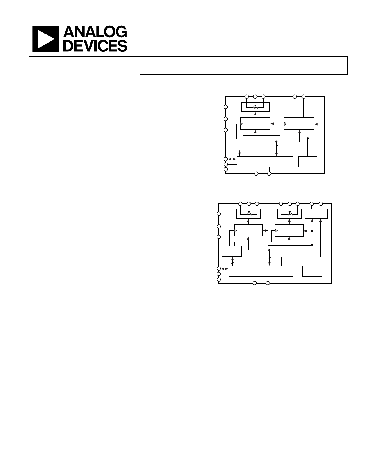
FUNCTIONAL BLOCK DIAGRAM
A1 W1 B1
O1 O2
SHDN
VDD
RDAC
REGISTER 1
REGISTER 2
VSS
ADDR
DECODE
AD5241
8
SDA
SCL
GND
SERIAL INPUT REGISTER
PWR-ON
RESET
AD0 AD1
Figure 1. AD5241 Functional Block Diagram
A1 W1 B1
A2 W2 B2
O1 O2
SHDN
REGISTER
VDD
RDAC
RDAC
REGISTER 1
REGISTER 2
VSS
SDA
SCL
GND
ADDR
DECODE
1
AD5242
8
SERIAL INPUT REGISTER
PWR-ON
RESET
AD0 AD1
Figure 2. AD5242 Functional Block Diagram
GENERAL DESCRIPTION
The AD5241/AD5242 provide a single-/dual-channel, 256-
position, digitally controlled variable resistor (VR) device. These
devices perform the same electronic adjustment function as a
potentiometer, trimmer, or variable resistor. Each VR offers a
completely programmable value of resistance between the A
terminal and the wiper, or the B terminal and the wiper. For the
AD5242, the fixed A-to-B terminal resistance of 10 kΩ, 100 kΩ,
or 1 MΩ has a 1% channel-to-channel matching tolerance. The
nominal temperature coefficient of both parts is 30 ppm/°C.
Wiper position programming defaults to midscale at system
power on. When powered, the VR wiper position is programmed
by an I2C®-compatible, 2-wire serial data interface. Both parts
have two extra programmable logic outputs available that
enable users to drive digital loads, logic gates, LED drivers, and
analog switches in their system.
The AD5241/AD5242 are available in surface-mount, 14-lead
SOIC and 16-lead SOIC packages and, for ultracompact solutions,
14-lead TSSOP and 16-lead TSSOP packages. All parts are
guaranteed to operate over the extended temperature range of
−40°C to +105°C.
Rev. C
Information furnished by Analog Devices is believed to be accurate and reliable. However, no
responsibility is assumed by Analog Devices for its use, nor for any infringements of patents or other
rights of third parties that may result from its use. Specifications subject to change without notice. No
license is granted by implication or otherwise under any patent or patent rights of Analog Devices.
Trademarksandregisteredtrademarksarethepropertyoftheirrespectiveowners.
One Technology Way, P.O. Box 9106, Norwood, MA 02062-9106, U.S.A.
Tel: 781.329.4700
www.analog.com
Fax: 781.461.3113 ©2001–2009 Analog Devices, Inc. All rights reserved.
1 page 
TIMING DIAGRAMS
t8
SDA
t1
t8 t9
t2
SCL
t2
PS
t3
t4
t6
t7 t5
S
Figure 3. Detail Timing Diagram
AD5241/AD5242
t10
P
Data of AD5241/AD5242 is accepted from the I2C bus in the following serial format.
Table 2.
S 0 1 0 1 1 AD1 AD0 R/W A A/B
Slave Address Byte
RS SD O1 O2 X X X A D7 D6 D5 D4 D3 D2 D1 D0 A P
Instruction Byte
Data Byte
where:
S = start condition
P = stop condition
A = acknowledge
X = don’t care
AD1, AD0 = Package pin programmable address bits. Must be matched with the logic states at Pins AD1 and AD0.
R/W = Read enable at high and output to SDA. Write enable at low.
A/B = RDAC subaddress select; 0 for RDAC1 and 1 for RDAC2.
RS = Midscale reset, active high.
SD = Shutdown in active high. Same as SHDN except inverse logic.
O1, O2 = Output logic pin latched values
D7, D6, D5, D4, D3, D2, D1, D0 = data bits.
SCL
SDA
START BY
MASTER
1 91 91 9
0 1 0 1 1 AD1 AD0 R/W
A/B RS SD O1 O2 X X X
D7 D6 D5 D4 D3 D2 D1 D0
FRAME 1
SLAVE ADDRESS BYTE
ACK BY
AD5241
FRAME 2
INSTRUCTION BYTE
ACK BY
AD5241
FRAME 3
DATA BYTE
ACK BY
AD5241
STOP BY
MASTER
Figure 4. Writing to the RDAC Serial Register
SCL
1
91
9
SDA
START BY
MASTER
0 1 0 1 1 AD1 AD0 R/W
D7 D6 D5 D4 D3 D2 D1 D0
FRAME 1
SLAVE ADDRESS BYTE
ACK BY
AD5241
NO ACK BY
MASTER
FRAME 2
DATA BYTE FROM PREVIOUSLY SELECTED
STOP BY
MASTER
RDAC REGISTER IN WRITE MODE
Figure 5. Reading Data from a Previously Selected RDAC Register in Write Mode
Rev. C | Page 5 of 20
5 Page 
AD5241/AD5242
TEST CIRCUITS
Figure 22 to Figure 30 define the test conditions used in the product specifications table.
5V
DUT
V+ A W
B
V1 +LS=BVD=DV+/2N
VMS
OFFSET
GND
OP279
VIN W
A DUT
OFFSET
BIAS
B
VOUT
Figure 22. Potentiometer Divider Nonlinearity Error (INL, DNL)
Figure 27. Noninverting Gain
NO CONNECT
DUT
A
W
B
IW
VMS
Figure 23. Resistor Position Nonlinearity Error
(Rheostat Operation; R-INL, R-DNL)
VMS2
DUT
AW
B
IW = VDD/RNOMINAL
VW
VMS1 RW = [VMS1 – VMS2]/IW
Figure 24. Wiper Resistance
A
VIN
OFFSET
GND
2.5V
DUT
B
W
+15V
OP42
–15V
Figure 28. Gain vs. Frequency
VOUT
DUT
W
B
RSW =
0.1V
ISW
CODE = 0x00
ISW 0.1V
VSS TO VDD
Figure 29. Incremental On Resistance
VA
VDD A
V+ W
B
V+ = VDD ±10%
PSRR (dB) = 20 LOG
ΔVMS
ΔVDD
PSS (%/%) =
ΔVMS%
ΔVDD%
VMS
Figure 25. Power Supply Sensitivity (PSS, PSRR)
NC
VDD
DUT
VSS
GND
A
W
B
ICM
VCM
NC
Figure 30. Common-Mode Leakage Current
OFFSET
GND
A DUT B
W
5V
OP279
OFFSET
BIAS
Figure 26. Inverting Gain
VOUT
Rev. C | Page 11 of 20
11 Page | ||
| Páginas | Total 20 Páginas | |
| PDF Descargar | [ Datasheet AD5242.PDF ] | |
Hoja de datos destacado
| Número de pieza | Descripción | Fabricantes |
| AD524 | Precision Instrumentation Amplifier | Analog Devices |
| AD5240 | FAST/ COMPLETE 12-BIT A/D CONVERTERS | Analog Devices |
| AD5241 | 2-Channel/ 256-Position Digital Potentiometer | Analog Devices |
| AD5242 | 2-Channel/ 256-Position Digital Potentiometer | Analog Devices |
| Número de pieza | Descripción | Fabricantes |
| SLA6805M | High Voltage 3 phase Motor Driver IC. |
Sanken |
| SDC1742 | 12- and 14-Bit Hybrid Synchro / Resolver-to-Digital Converters. |
Analog Devices |
|
DataSheet.es es una pagina web que funciona como un repositorio de manuales o hoja de datos de muchos de los productos más populares, |
| DataSheet.es | 2020 | Privacy Policy | Contacto | Buscar |