|
|
|
PDF AD7278 Data sheet ( Hoja de datos )
| Número de pieza | AD7278 | |
| Descripción | 12-/10-/8-Bit ADCs | |
| Fabricantes | Analog Devices | |
| Logotipo | ||
Hay una vista previa y un enlace de descarga de AD7278 (archivo pdf) en la parte inferior de esta página. Total 29 Páginas | ||
|
No Preview Available !
FEATURES
Throughput rate: 3 MSPS
Specified for VDD of 2.35 V to 3.6 V
Power consumption
12.6 mW at 3 MSPS with 3 V supplies
Wide input bandwidth
70 dB SNR at 1 MHz input frequency
Flexible power/serial clock speed management
No pipeline delays
High speed serial interface
SPI®-/QSPI™-/MICROWIRE™-/DSP-compatible
Temperature range: −40°C to +125°C
Power-down mode: 0.1 μA typical
6-lead TSOT package
8-lead MSOP package
AD7476 and AD7476A pin-compatible
GENERAL DESCRIPTION
The AD7276/AD7277/AD7278 are 12-/10-/8-bit, high speed,
low power, successive approximation analog-to-digital converters
(ADCs), respectively. The parts operate from a single 2.35 V
to 3.6 V power supply and feature throughput rates of up to
3 MSPS. The parts contain a low noise, wide bandwidth track-
and-hold amplifier that can handle input frequencies in excess
of 55 MHz.
The conversion process and data acquisition are controlled
using CS and the serial clock, allowing the devices to interface
with microprocessors or DSPs. The input signal is sampled on
the falling edge of CS, and the conversion is also initiated at this
point. There are no pipeline delays associated with the part.
The AD7276/AD7277/AD7278 use advanced design techniques
to achieve very low power dissipation at high throughput rates.
The reference for the part is taken internally from VDD. This
allows the widest dynamic input range to the ADC; therefore,
the analog input range for the part is 0 to VDD. The conversion
rate is determined by the SCLK.
3 MSPS, 12-/10-/8-Bit
ADCs in 6-Lead TSOT
AD7276/AD7277/AD7278
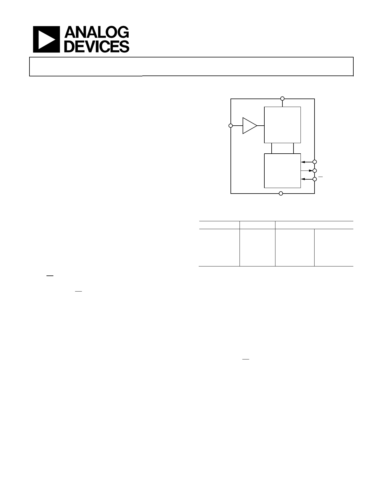
FUNCTIONAL BLOCK DIAGRAM
VDD
12-/10-/8-BIT
VIN
SUCCESSIVE
T/H APPROXIMATION
ADC
AD7276/
AD7277/
AD7278
CONTROL
LOGIC
SCLK
SDATA
CS
GND
Figure 1.
Table 1.
Part Number
AD7276
AD7277
AD7278
AD72741
AD72731
Resolution
12
10
8
12
10
Package
8-Lead MSOP 6-Lead TSOT
8-Lead MSOP 6-Lead TSOT
8-Lead MSOP 6-Lead TSOT
8-Lead MSOP 8-Lead TSOT
8-Lead MSOP 8-Lead TSOT
1 Part contains external reference pin.
PRODUCT HIGHLIGHTS
1. 3 MSPS ADCs in a 6-lead TSOT package.
2. AD7476/AD7477/AD7478 and AD7476A/AD7477A/
AD7478A pin-compatible.
3. High throughput with low power consumption.
4. Flexible power/serial clock speed management. This allows
maximum power efficiency at low throughput rates.
5. Reference derived from the power supply.
6. No pipeline delay. The parts feature a standard successive
approximation ADC with accurate control of the sampling
instant via a CS input and once-off conversion control.
Rev. C
Information furnished by Analog Devices is believed to be accurate and reliable. However, no
responsibility is assumed by Analog Devices for its use, nor for any infringements of patents or other
rights of third parties that may result from its use. Specifications subject to change without notice. No
license is granted by implication or otherwise under any patent or patent rights of Analog Devices.
Trademarksandregisteredtrademarksarethepropertyoftheirrespectiveowners.
One Technology Way, P.O. Box 9106, Norwood, MA 02062-9106, U.S.A.
Tel: 781.329.4700
www.analog.com
Fax: 781.461.3113 © 2005–2011 Analog Devices, Inc. All rights reserved.
1 page 
AD7276/AD7277/AD7278
Parameter
CONVERSION RATE
Conversion Time
Track-and-Hold Acquisition Time4
Throughput Rate
POWER REQUIREMENTS
VDD
IDD
Normal Mode (Static)
Normal Mode (Operational)
Partial Power-Down Mode (Static)
Full Power-Down Mode (Static)
Power Dissipation6
Normal Mode (Operational)
Partial Power-Down
Full Power-Down
A Grade2, 3
291
875
60
3
2.35/3.6
1
5.5
2.5
4.2
1.6
34
2
10
19.8
9
12.6
4.8
102
7.2
1 Y Grade specifications are guaranteed by characterization.
2 Temperature range from −40°C to +125°C.
3 Typical specifications are tested with VDD = 3 V and at 25°C.
4 See the Terminology section.
5 Guaranteed by characterization.
6 See the Power vs. Throughput Rate section.
B, Y Grade2,3 Unit
Test Conditions/Comments
291
ns max
14 SCLK cycles with SCLK at 48 MHz, B Grade
875
ns max
14 SCLK cycles with SCLK at 16 MHz, Y Grade
60 ns min
3 MSPS max See the Serial Interface section
2.35/3.6
1
5.5
2.5
4.2
1.6
34
2
10
V min/max
mA typ
mA max
mA max
mA typ
mA typ
μA typ
μA max
μA max
Digital I/Ps 0 V or VDD
VDD = 3.6 V, SCLK on or off
VDD = 2.35 V to 3.6 V, fSAMPLE = 3 MSPS, B Grade
VDD = 2.35 V to 3.6 V, fSAMPLE = 1 MSPS, Y Grade
VDD = 3 V, fSAMPLE = 3 MSPS, B Grade
VDD = 3 V, fSAMPLE = 1 MSPS, Y Grade
−40°C to +85°C, typically 0.1 μA
85°C to 125°C
19.8
mW max
VDD = 3.6 V, fSAMPLE = 3 MSPS, B Grade
9
mW max
VDD = 3.6 V, fSAMPLE = 1 MSPS, Y Grade
12.6
mW typ
VDD = 3 V, fSAMPLE = 3 MSPS, B Grade
4.8
mW typ
VDD = 3 V, fSAMPLE = 1 MSPS, Y Grade
102
μW typ
VDD = 3 V
7.2
μW max
VDD = 3.6 V, −40°C to +85°C
Rev. C | Page 4 of 28
5 Page 
AD7276/AD7277/AD7278
TIMING EXAMPLES
For the AD7276, if CS is brought high during the 14th SCLK rising
edge after the two leading zeros and 12 bits of the conversion
have been provided, the part can achieve the fastest throughput
rate, 3 MSPS. If CS is brought high during the 16th SCLK rising
edge after the two leading zeros and 12 bits of the conversion
and two trailing zeros have been provided, a throughput rate of
2.97 MSPS is achievable. This is illustrated in the following two
timing examples.
Timing Example 1
In Figure 6, using a 14 SCLK cycle, fSCLK = 48 MHz and the
throughput is 3 MSPS. This produces a cycle time of t2 +
12.5(1/fSCLK) + tACQ = 333 ns, where t2 = 6 ns minimum and
tACQ = 67 ns.
This satisfies the requirement of 60 ns for tACQ. Figure 6 also
shows that tACQ comprises 0.5(1/fSCLK) + t8 + tQUIET, where
t8 = 14 ns max. This allows a value of 43 ns for tQUIET, satisfying
the minimum requirement of 4 ns.
Timing Example 2
The example in Figure 7 uses a 16 SCLK cycle, fSCLK = 48 MHz,
and the throughput is 2.97 MSPS. This produces a cycle time of
t2 + 12.5(1/fSCLK) + tACQ = 336 ns, where t2 = 6 ns minimum and
tACQ = 70 ns. Figure 7 shows that tACQ comprises 2.5(1/fSCLK) + t8 +
tQUIET, where t8 = 14 ns max. This satisfies the minimum
requirement of 4 ns for tQUIET.
t1
CS
SCLK
t2
1
tCONVERT
t6
2 345
t3
SDATA
Z ZERO
THREE-
STATE
2 LEADING
ZEROS
DB11
DB10
t4
DB9
B
13
t7
DB1 DB0
1/THROUGHPUT
14 15 16
t5 t8
ZERO ZERO
2 TRAILING
ZEROS
tQUIET
THREE-STATE
Figure 5. AD7276 Serial Interface Timing Diagram
CS
SCLK
t2
1
tCONVERT
t6
234
t3
SDATA THREE-
STATE
Z ZERO
2 LEADING
ZEROS
DB11
DB10
t4
DB9
5
t7
B
13
t5
14
t9
DB1
DB0
1/THROUGHPUT
t1
tQUIET
THREE-STATE
Figure 6. AD7276 Serial Interface Timing 14 SCLK Cycle
CS
SCLK
t1
tCONVERT
t2
B
1 2 3 4 5 12 13 14 15 16
12.5(1/fSCLK)
1/THROUGHPUT
t8
tACQUISITION
tQUIET
Figure 7. AD7276 Serial Interface Timing 16 SCLK Cycle
Rev. C | Page 10 of 28
11 Page | ||
| Páginas | Total 29 Páginas | |
| PDF Descargar | [ Datasheet AD7278.PDF ] | |
Hoja de datos destacado
| Número de pieza | Descripción | Fabricantes |
| AD7273 | 10-/12-Bit ADCs | Analog Devices |
| AD7274 | 10-/12-Bit ADCs | Analog Devices |
| AD7276 | 12-/10-/8-Bit ADCs | Analog Devices |
| AD7277 | 12-/10-/8-Bit ADCs | Analog Devices |
| Número de pieza | Descripción | Fabricantes |
| SLA6805M | High Voltage 3 phase Motor Driver IC. |
Sanken |
| SDC1742 | 12- and 14-Bit Hybrid Synchro / Resolver-to-Digital Converters. |
Analog Devices |
|
DataSheet.es es una pagina web que funciona como un repositorio de manuales o hoja de datos de muchos de los productos más populares, |
| DataSheet.es | 2020 | Privacy Policy | Contacto | Buscar |