|
|
|
PDF AD6622 Data sheet ( Hoja de datos )
| Número de pieza | AD6622 | |
| Descripción | Four-Channel/ 75 MSPS Digital Transmit Signal Processor TSP | |
| Fabricantes | Analog Devices | |
| Logotipo | ||
Hay una vista previa y un enlace de descarga de AD6622 (archivo pdf) en la parte inferior de esta página. Total 28 Páginas | ||
|
No Preview Available !
a
FEATURES
Wideband Digital IF Parallel Output
Wideband Digital IF Parallel Input
Allows Cascade of Chips for Additional Channels
Programmable IF and Modulation for Each Channel
Programmable Interpolating RAM Coefficient Filter
High-Speed CIC Interpolating Filter
NCO Frequency Translation
Worst Spur Better than 100 dBc
Tuning Resolution Better than 0.02 Hz
Real or Complex Outputs
Digital Summation of Channels
Clipped or Wrapped Overrange
Two’s Complement or Offset Binary Output
Separate 3-Wire Serial Data Input for Each Channel
Microprocessor Control
JTAG Boundary Scan
APPLICATIONS
Cellular/PCS Base Stations
Micro/Pico Cell Base Stations
WBCDMA
Wireless Local Loop Base Stations
Phase Array Beam Forming Antennas
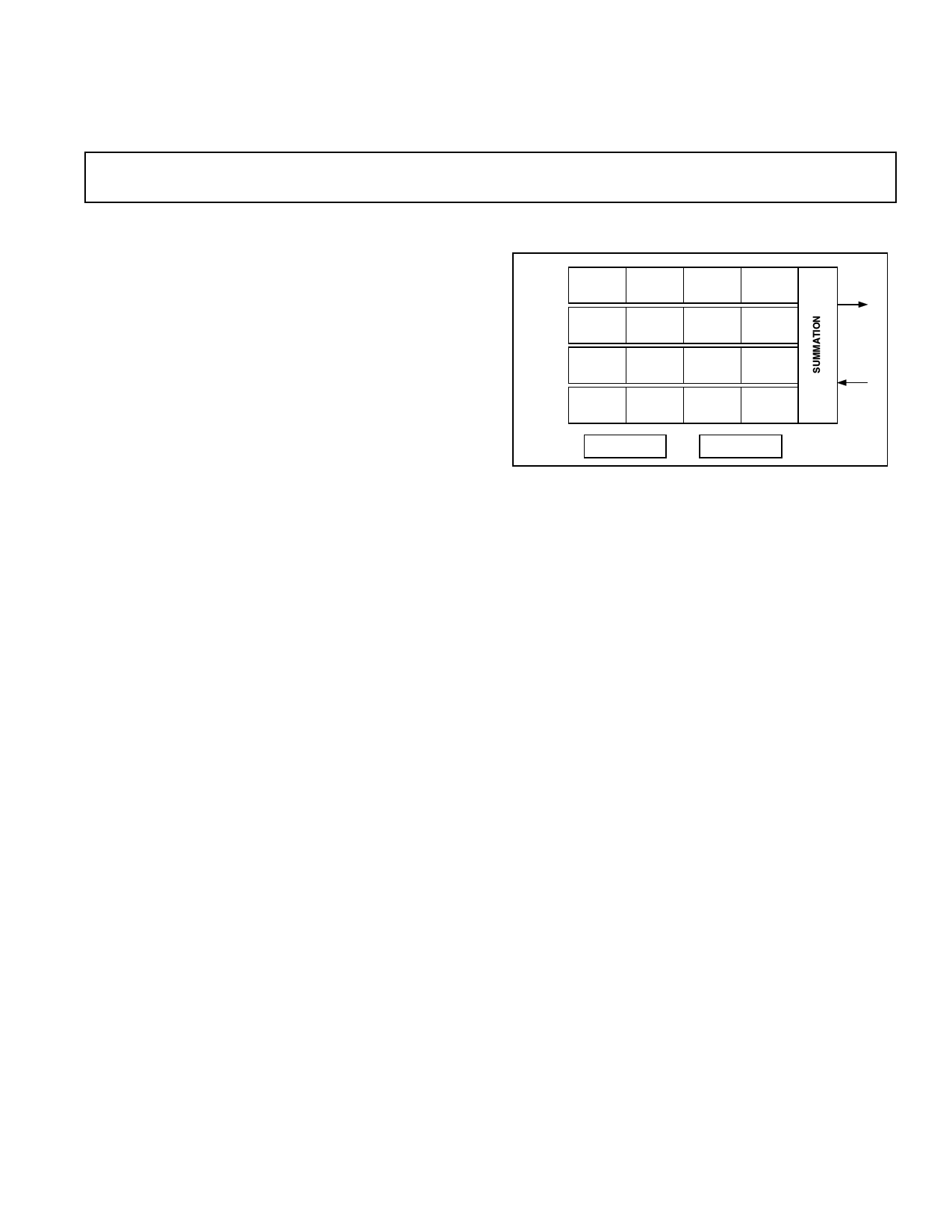
Four-Channel, 75 MSPS Digital
Transmit Signal Processor (TSP)
AD6622
FUNCTIONAL BLOCK DIAGRAM
CH A SPORT
RCF
CH B SPORT
RCF
CH C SPORT
RCF
CH D SPORT
RCF
JTAG
CIC
FILTER
CIC
FILTER
CIC
FILTER
CIC
FILTER
NCO
NCO
NCO
NCO
PORT
18
18
PRODUCT DESCRIPTION
The AD6622 comprises four identical digital Transmit Signal
Processors (TSPs) complete with synchronization circuitry and
cascadable wideband channel summation. An external digital-
to-analog converter (DAC) is all that is required to complete a
wide band digital up-converter. On-chip tuners allow the relative
phase and frequency for each RF carrier to be independently
controlled.
Each TSP has three cascaded signal processing elements: a
RAM-programmable Coefficient interpolating Filter (RCF), a
programmable Cascaded Integrator Comb (CIC) interpolating
filter, and a Numerically Controlled Oscillator/tuner (NCO).
The outputs of the four TSPs are summed and scaled on-chip.
In multichannel wideband transmitters, multiple AD6622s may
be combined using the chip’s cascadable output summation stage.
Each channel provides independent serial data inputs that may
be directly connected to the serial port of DSP chips. User pro-
grammable FIR filters can be used to filter linear inputs.
All control registers and coefficient values are programmed through
a generic microprocessor interface. Two microprocessor bus
modes are supported. All inputs and outputs are LVCMOS
compatible. All outputs are LVCMOS and 5 V TTL compatible.
REV. 0
Information furnished by Analog Devices is believed to be accurate and
reliable. However, no responsibility is assumed by Analog Devices for its
use, nor for any infringements of patents or other rights of third parties
which may result from its use. No license is granted by implication or
otherwise under any patent or patent rights of Analog Devices.
One Technology Way, P.O. Box 9106, Norwood, MA 02062-9106, U.S.A.
Tel: 781/329-4700 World Wide Web Site: http://www.analog.com
Fax: 781/326-8703
© Analog Devices, Inc., 2000
1 page 
RD (DS)
WR (R/W)
tHWR
AD6622
CS
A[2:0]
D[7:0]
RDY
(DTACK)
tSAM
VALID ADDRESS
tSAM
VALID DATA
tDRDY
tACC
tHAM
tHAM
1. tACC ACCESS TIME DEPENDS ON THE ADDRESS ACCESSED. ACCESS TIME IS MEASURED FROM THE FE OF WR TO THE RE OF RDY.
2. tACCFAST REQUIRES A MAXIMUM OF THREE CLK PERIODS AND APPLIES TO A[2:0] = 7, 6, 5, 3, 2, 1
3. tACCMEDIUM REQUIRES A MAXIMUM OF FOUR CLK PERIODS AND APPLIES TO A[2:0] = 4 AND 0 IF THE ACCESS IS TO A CONTROL REGISTER
VERSUS A RAM REGISTER.
4. tACCSLOW REQUIRES A MAXIMUM OF FIVE CLK PERIODS AND APPLIES TO A[2:0] = 0 WHEN ACCESSING RAM REGISTERS.
Figure 5. INM Microport Write Timing Requirements
RD (DS)
WR (R/W)
CS
A[2:0]
D[7:0]
RDY
(DTACK)
tSAM
tZD
tDRDY
tACC
VALID ADDRESS
tDD tHA
VALID DATA
tZD
1. tACC ACCESS TIME DEPENDS ON THE ADDRESS ACCESSED. ACCESS TIME IS MEASURED FROM THE FE OF WR TO THE RE OF RDY.
2. tACCFAST REQUIRES A MAXIMUM OF THREE CLK PERIODS AND APPLIES TO A[2:0] = 7, 6, 5, 3, 2, 1
3. tACCMEDIUM REQUIRES A MAXIMUM OF FOUR CLK PERIODS AND APPLIES TO A[2:0] = 4 AND 0 IF THE ACCESS IS TO A CONTROL REGISTER
VERSUS A RAM REGISTER.
4. tACCSLOW REQUIRES A MAXIMUM OF FIVE CLK PERIODS AND APPLIES TO A[2:0] = 0 WHEN ACCESSING RAM REGISTERS.
Figure 6. INM Microport Read Timing Requirements
REV. 0
–5–
5 Page 
AD6622
The serial data frame sync output, SDFS, is pulsed high for one
SCLK cycle at the input sample rate. The input sample rate is
determined by the master clock divided by channel interpolation
factor. If the SCLK rate is not an integer multiple of the input
sample rate, the SDFS will continually adjust the period by one
SCLK cycle in order to keep the average SDFS rate equal to the
input sample rate. When the channel is in sleep mode, SDFS is
held low. The first SDFS is delayed by the channel reset latency
after the Channel Reset is removed. The channel reset latency
varies dependent on channel configuration.
The serial data input, SDIN, accepts 32-bit words as channel
input data. The 32-bit word is interpreted as two 16 bit two’s
complement quadrature words, I followed by Q, MSB first.
The first bit is shifted into the serial port starting on the second
rising edge of SCLK after SDFS goes high, as shown by the
timing diagram below.
CLK
SCLK
SDFS
SDI
tDSCLK
tDSDFS
tDSDFS
CLKn
tSSI tHSI
DATAn
Figure 10. Serial Port Switching Characteristics
As an example of the serial port operation, consider a CLK fre-
quency of 62.208 MSPS and a channel interpolation of 2560.
In that case, the input sample rate is 24.3 kSPS (62.208 MSPS/
2560), which is also the SDFS rate. Substituting, fSCLK ≥ 32 ×
fSDFS into the equation below and solving for SCLKDIVIDER,
we find the maximum value for SCLKDIVIDER according to
Equation 2.
f
SCLK DIVIDER
≤
CLK
64 × f
–1
SDFS
(2)
Evaluating this equation for our example, SCLKDIVIDER must be
less than or equal to 39. Since the SCLKDIVIDER channel regis-
ter is a 5-bit unsigned number it can only range from 0 to 31.
Any value in that range will be valid for this example, but if it is
important that the SDFS period is constant, then there is another
restriction. For regular frames, the ratio fSCLK/fSDFS must be equal
to an integer of 32 or larger. For this example, constant SDFS
periods can only be achieved with an SCLK divider of 19.
In conclusion, the SDFS rate is determined by the AD6622 master
clock rate and the interpolation rate of the channel. The SDFS
rate is equal to the channel input rate. The channel interpola-
tion is equal to RCF interpolation times CIC5 interpolation,
times CIC2 interpolation
L = LRCF × LCIC5 × LCIC2
(3)
The SCLK rate is determined by the AD6622 master clock
rate and SCLKDIVIDER. The SCLK is a divided version of the
AD6622 master CLK. The SCLK divide ratio is determined by
SCLKDIVIDER as shown in Equation 2. The SCLK must be fast
enough to input 32 bits of data prior to the next SDFS. Extra
SCLKs are ignored by the serial port.
PROGRAMMABLE INTERPOLATING RAM
COEFFICIENT FILTER (RCF)
Each channel has a fully independent RAM Coefficient Filter
(RCF). The RCF accepts data from the serial port, filters it, and
passes the result to the CIC filter. The RCF implements a FIR
filter with optional interpolation. The FIR filter can produce
impulse responses up to 128 output samples long. The FIR
response may be interpolated up to a factor of 128, although
the best filter performance is usually achieved if the RCF inter-
polation factor is confined to 8 or below.
FIR Filter Implementation
The RCF accepts quadrature samples from the serial port with a
fixed point resolution of 16 bits each, for I and Q.
SDFS
SCLK
SDIN
SERIAL
PORT
DATA
MEM
16,16
16,16
COEFFICIENT
MEM
RCF
ACCUMULATOR
16,16 IQ TO
CIC
FILTER
RCF COARSE
SCALE
Figure 11. RCF Block Diagram
The AD6622 RCF realizes a sum-of-products filter using a poly-
phase implementation. This mode is equivalent to an interpola-
tor followed by a FIR filter running at the interpolated rate. In
Figure 12, the interpolating block increases the rate by the RCF
interpolation factor (LRCF) by inserting LRCF-1 zero valued samples
between every input sample. The next block is a filter with a finite
impulse response length (NRCF) and an impulse response of h[n],
where n is an integer from 0 to NRCF-1.
fIN fIN ؋ LRCF NRCF TAP fIN ؋ LRCF
LRCF
FIR FILTER
a b h[n] c
Figure 12. RCF Interpolation
The difference equation for Figure 12 is written below, where
h[n] is the RCF impulse response, b[n] is the interpolated input
sample sequence at point “b” in Figure 12, and c[n] is the out-
put sample sequence at point “c” in the Figure 12.
NRCF −1
c[n] = ∑ h[k − n] × b[n]
k=0
(4)
This difference equation can be described by the transfer func-
tion from point “b” to “c” as shown Equation 5.
NRCF −1
Hbc(z) = ∑ h[n] × z−n
n=0
(5)
The actual implementation of this filter uses a polyphase
decomposition to skip the multiply-accumulates when b[n] is
zero. Compared to the diagram above, this implementation has
the benefits of reducing by a factor of LRCF both the time needed to
calculate an output and the required data memory (DMEM). The
price of these benefits is that the user must place the coefficients
into the coefficient memory (CMEM) indexed by the interpo-
lation phase. The process of selecting the coefficients and placing
them into the CMEM is broken into three steps shown below.
REV. 0
–11–
11 Page | ||
| Páginas | Total 28 Páginas | |
| PDF Descargar | [ Datasheet AD6622.PDF ] | |
Hoja de datos destacado
| Número de pieza | Descripción | Fabricantes |
| AD6620 | 65 MSPS Digital Receive Signal Processor | Analog Devices |
| AD6622 | Four-Channel/ 75 MSPS Digital Transmit Signal Processor TSP | Analog Devices |
| AD6623 | 4-Channel/ 104 MSPS Digital Transmit Signal Processor TSP | Analog Devices |
| AD6624 | 80 MSPS Digital Receive Signal Processor | Analog Devices |
| Número de pieza | Descripción | Fabricantes |
| SLA6805M | High Voltage 3 phase Motor Driver IC. |
Sanken |
| SDC1742 | 12- and 14-Bit Hybrid Synchro / Resolver-to-Digital Converters. |
Analog Devices |
|
DataSheet.es es una pagina web que funciona como un repositorio de manuales o hoja de datos de muchos de los productos más populares, |
| DataSheet.es | 2020 | Privacy Policy | Contacto | Buscar |