|
|
|
PDF AD6432 Data sheet ( Hoja de datos )
| Número de pieza | AD6432 | |
| Descripción | GSM 3 V Transceiver IF Subsystem | |
| Fabricantes | Analog Devices | |
| Logotipo | ||
Hay una vista previa y un enlace de descarga de AD6432 (archivo pdf) en la parte inferior de esta página. Total 20 Páginas | ||
|
No Preview Available !
a
GSM 3 V Transceiver IF Subsystem
AD6432
FEATURES
Fully Compliant with Standard and Enhanced GSM
Specification
DC-350 MHz RF Bandwidths
80 dB Gain Control Range
I/Q Modulation and Demodulation
Onboard Phase Locked Tunable Oscillator
On-Chip Noise Roofing IF Filters
Ultralow Power Design
2.7 V–3.6 V Operating Voltage
User-Selectable Power-Down Modes
Small 44-Lead TQFP Package
Interfaces Directly with AD20msp410 and AD20msp415
GSM Baseband Chipsets
APPLICATIONS
I/Q Modulated Digital Wireless Systems
GSM Mobile Radios
GSM PCMCIA Cards
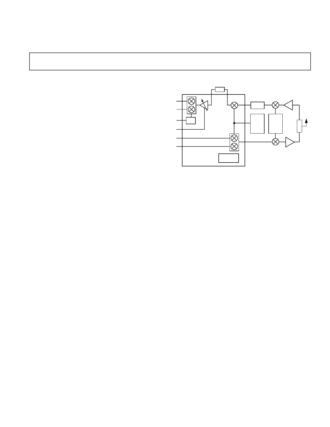
FUNCTIONAL BLOCK DIAGRAM
BP
PLO
SAW
IF
SYNTH
RF
SYNTH
AD6432
OP AMP
PA
GENERAL DESCRIPTION
The AD6432 IF IC provides the complete transmit and receive
IF signal processing, including I/Q modulation and demodula-
tion, necessary to implement a digital wireless transceiver such
as a GSM handset. The AD6432 may also be used for other
wireless TDMA standards using I/Q modulation.
The AD6432’s receive signal path is based on the proven archi-
tecture of the AD607 and the AD6459. It consists of a mixer,
gain-controlled amplifiers, integrated roofing filter and I/Q
demodulators based on a PLL. The low noise, high-intercept
variable-gain mixer is a doubly-balanced Gilbert-cell type. It has
a nominal –13 dBm input-referred 1 dB compression point and
a 0 dBm input-referred third-order intercept.
The gain-control input accepts an external control voltage input
from an external AGC detector or a DAC. It provides an 80 dB
gain range with 27.5 mV/dB gain scaling, where the mixer and
the IF gains vary together.
The I and Q demodulators provide inphase and quadrature
baseband outputs to interface with Analog Devices’ AD7015
and AD6421 (GSM, DCS1800, PCS1900) baseband convert-
ers. An onboard quadrature VCO, externally phase-locked to
the IF signal, drives the I and Q demodulators. The quadrature
phase-locked oscillator (QPLO) requires no external compo-
nents for frequency control or quadrature generation, and de-
modulates signals at standard GSM system IFs of 13 MHz, or
26 MHz with a reference input frequency of 13 MHz; or, in
general, 1X or 2X the reference frequency. Maximum reference
frequency is 25 MHz.
This reference signal is normally provided by an external
VCTCXO under the control of the radio’s digital signal
processor. The transmit path consists of an I/Q modulator
and buffer amplifier, suitable for carrier frequencies up to
300 MHz and provides an output power of –17.5 dBm in
a 50 Ω system. The quadrature LO signals driving the
I and Q modulator are generated internally by dividing by
two the frequency of the signal presented at the differential
LO port of the AD6432. In both the transmit and receive
paths, onboard filters provide 30 dB of stopband attenuation.
The AD6432 comes in a 44-lead plastic thin quad flatpack
(TQFP) surface mount package.
REV. 0
Information furnished by Analog Devices is believed to be accurate and
reliable. However, no responsibility is assumed by Analog Devices for its
use, nor for any infringements of patents or other rights of third parties
which may result from its use. No license is granted by implication or
otherwise under any patent or patent rights of Analog Devices.
One Technology Way, P.O. Box 9106, Norwood, MA 02062-9106, U.S.A.
Tel: 617/329-4700 World Wide Web Site: http://www.analog.com
Fax: 617/326-8703
© Analog Devices, Inc., 1997
1 page 
AD6432
PCAP
TXPU
QTXN
C9
0.1 F
R30
49.9Ω
R11
1kΩ
R10
500Ω
VS1
QTXP
ITXN
ITXP
VS1
VPTX
DECOUPLING
R12
0Ω
C28
0.1 F
C5
0.01 F
R39
OPEN
R25
1kΩ
MODO
VS1
VPDV
DECOUPLING
R2
0Ω
C29
0.1 F
LOLO
6 T1 1 C18
0.1 F
2
43
R9
84Ω
C14
0.01 F
R14
249Ω
RFHI
C1
100pF
R3
49.9Ω
C2
100pF
R23
123Ω
C15
100pF
44 43 42 41 40 39 38 37 36 35 34
GND 1
MODO 2
VPDV 3
CMTX 4
LOLO 5
LOHI 6
CMRX 7
GND 8
RFLO 9
RFHI 10
GND 11
AD6432
TOP VIEW
(Pins Down)
33 FREF
32 GND
31 IFS0
30 CMDM
29 FLTR
28 VPFL
27 VPDM
26 IRXP
25 IRXN
24 QRXP
23 QRXN
12 13 14 15 16 17 18 19 20 21 22
TXPU
J1 VS2
C7
4.7 F
IFS0
RXPU
VS1
C7
4.7 F
J3
J4
J5
GREF
GAIN
GND
VS1
C30
0.1 F
R31
0Ω
C3
0.01 F
MXHI
MXLO
C43
0.047 F
C44
0.047 F
IFLO
C4
0.047 F
R4
49.9Ω
GREF
C39
0.01 F
C40
0.01 F
GAIN
RXPU
C7
0.047 F
R5
49.9Ω
IFHI
PCAM
R34
0Ω
R8
0Ω
C11
0.01 F
PCAO
C32
0.1 F
VS2
VPPC
DECOUPLING
C36
1000pF
C10 R1
1000pF 1kΩ
IFS0
R32
49.9Ω
R7
0Ω
C23
0.01 F
FREF
VS1
R6
0Ω
C41
0.01 F
C17
0.1 F
C6
47pF
IRXP
IRXN
C8
47pF
QRXP
QXRN
Figure 1. Characterization Board
REV. 0
–5–
5 Page 
PRODUCT OVERVIEW
The AD6432 provides most of the active circuitry required to
realize a complete low power, single-conversion superhetero-
dyne time division transceiver, or the latter part of a double-
conversion transceiver, at input receive frequencies up to
350 MHz with an IF from 10 MHz to 50 MHz and transmit
frequencies up to 300 MHz. The internal I/Q demodulators,
with their associated phase-locked loop and the internal I/Q
modulator, support a wide variety of modulation modes, includ-
ing n-PSK, n-QAM, and GMSK. A single positive supply volt-
age of 3 V is required (2.7 V minimum, 3.6 V maximum) at a
typical supply current of 13 mA at midgain in receive mode and
13 mA in transmit mode. In the following discussion, VPOS will
be used to denote the power supply voltage, which will be as-
sumed to be 3 V.
AD6432
Figure 27 shows the main sections of the AD6432. In the re-
ceive path, it consists of a variable-gain UHF mixer and linear
two-stage IF strip, both of which together provide a calibrated
voltage-controlled gain range of more than 80 dB, followed by a
tunable IF bandpass filter and dual quadrature demodulators.
These are driven by inphase and quadrature clocks generated
by a Phase-Locked Loop (PLL) locked to a corrected external
reference. In the transmit path it consists of a quadrature modu-
lator followed by a low-pass filter. The quadrature modulator is
driven by quadrature frequencies that are generated internally
by dividing the external local oscillator frequency by two. A
CMOS-compatible power-down interface completes the AD6432.
RFHI 10
RFLO 9
MXOP
13
14
MXOM
LC
BANDPASS
FILTER
IFIP
16
17
IFIM
LOHI 6
LOLO 5
2
0
90
MODO 2
PCAO 35
GAIN TEMP. COMPENSATION
AD6432
3MHz
90 0
QUADRATURE
VCO
DIVIDE BY
1 OR 2
PHASE
DETECTOR
RX, TX
BIAS
4.7kΩ
4.7kΩ
4.7kΩ
4.7kΩ
25 IRXN
26 IRXP
23 QRXN
24 QRXP
31 IFS0
33 FREF
29 FLTR
20 GAIN
21 GREF
19 RXPU
39 TXPU
42 ITXN
43 ITXP
40 QTXN
41 QTXP
38 PCAP
37 PCAM
Figure 27. Functional Block Diagram
REV. 0
–11–
11 Page | ||
| Páginas | Total 20 Páginas | |
| PDF Descargar | [ Datasheet AD6432.PDF ] | |
Hoja de datos destacado
| Número de pieza | Descripción | Fabricantes |
| AD6432 | GSM 3 V Transceiver IF Subsystem | Analog Devices |
| AD6439 | Discrete Multitone (DMT) Coprocessor | Analog Devices |
| Número de pieza | Descripción | Fabricantes |
| SLA6805M | High Voltage 3 phase Motor Driver IC. |
Sanken |
| SDC1742 | 12- and 14-Bit Hybrid Synchro / Resolver-to-Digital Converters. |
Analog Devices |
|
DataSheet.es es una pagina web que funciona como un repositorio de manuales o hoja de datos de muchos de los productos más populares, |
| DataSheet.es | 2020 | Privacy Policy | Contacto | Buscar |