|
|
|
PDF AD600 Data sheet ( Hoja de datos )
| Número de pieza | AD600 | |
| Descripción | Dual/ Low Noise/ Wideband Variable Gain Amplifiers | |
| Fabricantes | Analog Devices | |
| Logotipo | ||
Hay una vista previa y un enlace de descarga de AD600 (archivo pdf) en la parte inferior de esta página. Total 20 Páginas | ||
|
No Preview Available !
a
Dual, Low Noise, Wideband
Variable Gain Amplifiers
AD600/AD602*
FEATURES
Two Channels with Independent Gain Control
“Linear in dB” Gain Response
Two Gain Ranges:
AD600: 0 dB to +40 dB
AD602: –10 dB to +30 dB
Accurate Absolute Gain: ؎0.3 dB
Low Input Noise: 1.4 nV/√Hz
Low Distortion: –60 dBc THD at ؎1 V Output
High Bandwidth: DC to 35 MHz (–3 dB)
Stable Group Delay: ؎2 ns
Low Power: 125 mW (max) per Amplifier
Signal Gating Function for Each Amplifier
Drives High Speed A/D Converters
MIL-STD-883 Compliant and DESC Versions Available
APPLICATIONS
Ultrasound and Sonar Time-Gain Control
High Performance Audio and RF AGC Systems
Signal Measurement
PRODUCT DESCRIPTION
The AD600 and AD602 dual channel, low noise variable gain
amplifiers are optimized for use in ultrasound imaging systems,
but are applicable to any application requiring very precise gain,
low noise and distortion, and wide bandwidth. Each indepen-
dent channel provides a gain of 0 dB to +40 dB in the AD600
and –10 dB to +30 dB in the AD602. The lower gain of the
AD602 results in an improved signal-to-noise ratio at the out-
put. However, both products have the same 1.4 nV/√Hz input
noise spectral density. The decibel gain is directly proportional
to the control voltage, is accurately calibrated, and is supply-
and temperature-stable.
To achieve the difficult performance objectives, a proprietary
circuit form—the X-AMP®—has been developed. Each channel
of the X-AMP comprises a variable attenuator of 0 dB to
–42.14 dB followed by a high speed fixed gain amplifier. In this
way, the amplifier never has to cope with large inputs, and can
benefit from the use of negative feedback to precisely define the
gain and dynamics. The attenuator is realized as a seven-stage
R-2R ladder network having an input resistance of 100 Ω, laser-
trimmed to ± 2%. The attenuation between tap points is 6.02 dB;
the gain-control circuit provides continuous interpolation be-
tween these taps. The resulting control function is linear in dB.
X-AMP is a registered trademark of Analog Devices, Inc.
*Patented.
FUNCTIONAL BLOCK DIAGRAM
SCALING
REFERENCE
PRECISION PASSIVE
INPUT ATTENUATOR
GAT1
GATING
INTERFACE
C1HI
C1LO
VG
GAIN CONTROL
INTERFACE
A1HI
A1LO
0dB –6.02dB –12.04dB –18.06dB –22.08dB –30.1dB –36.12dB –42.14dB
500Ω
R – 2R LADDER NETWORK
62.5Ω
RF2
2.24kΩ (AD600)
694Ω (AD602)
RF1
20Ω
FIXED GAIN
AMPLIFIER
41.07dB (AD600)
31.07dB (AD602)
A1OP
A1CM
The gain-control interfaces are fully differential, providing an
input resistance of ~15 MΩ and a scale factor of 32 dB/V (that
is, 31.25 mV/dB) defined by an internal voltage reference. The
response time of this interface is less than 1 µs. Each channel
also has an independent gating facility that optionally blocks sig-
nal transmission and sets the dc output level to within a few mil-
livolts of the output ground. The gating control input is TTL
and CMOS compatible.
The maximum gain of the AD600 is 41.07 dB, and that of the
AD602 is 31.07 dB; the –3 dB bandwidth of both models is
nominally 35 MHz, essentially independent of the gain. The
signal-to-noise ratio (SNR) for a 1 V rms output and a 1 MHz
noise bandwidth is typically 76 dB for the AD600 and 86 dB for
the AD602. The amplitude response is flat within ± 0.5 dB from
100 kHz to 10 MHz; over this frequency range the group delay
varies by less than ± 2 ns at all gain settings.
Each amplifier channel can drive 100 Ω load impedances with
low distortion. For example, the peak specified output is ± 2.5 V
minimum into a 500 Ω load, or ± 1 V into a 100 Ω load. For a
200 Ω load in shunt with 5 pF, the total harmonic distortion for
a ± 1 V sinusoidal output at 10 MHz is typically –60 dBc.
The AD600J and AD602J are specified for operation from 0°C
to +70°C, and are available in both 16-pin plastic DIP (N) and
16-pin SOIC (R). The AD600A and AD602A are specified for
operation from –40°C to +85°C and are available in both 16-pin
cerdip (Q) and 16-pin SOIC (R).
The AD600S and AD602S are specified for operation from
–55°C to +125°C and are available in a 16-pin cerdip (Q) pack-
age and are MIL-STD-883 compliant. The AD600S and
AD602S are also available under DESC SMD 5962-94572.
REV. A
Information furnished by Analog Devices is believed to be accurate and
reliable. However, no responsibility is assumed by Analog Devices for its
use, nor for any infringements of patents or other rights of third parties
which may result from its use. No license is granted by implication or
otherwise under any patent or patent rights of Analog Devices.
One Technology Way, P.O. Box 9106, Norwood, MA 02062-9106, U.S.A.
Tel: 617/329-4700
Fax: 617/326-8703
1 page 
AD600/AD602
The Gain-Control Interface
The attenuation is controlled through a differential, high imped-
ance (15 MΩ) input, with a scaling factor which is laser
trimmed to 32 dB per volt, that is, 31.25 mV/dB. Each of the
two amplifiers has its own control interface. An internal band-
gap reference ensures stability of the scaling with respect to
supply and temperature variations, and is the only circuitry
common to both channels.
When the differential input voltage VG = 0 V, the attenuator
“slider” is centered, providing an attenuation of 21.07 dB, thus
resulting in an overall gain of 20 dB (= –21.07 dB + 41.07 dB).
When the control input is –625 mV, the gain is lowered by
20 dB (= 0.625 × 32), to 0 dB; when set to +625 mV, the gain
is increased by 20 dB, to 40 dB. When this interface is over-
driven in either direction, the gain approaches either –1.07 dB
(= –42.14 dB + 41.07 dB) or 41.07 dB (= 0 + 41.07 dB),
respectively.
The gain of the AD600 can thus be calculated using the follow-
ing simple expression:
Gain (dB) = 32 VG + 20
(1)
where VG is in volts. For the AD602, the expression is:
Gain (dB) = 32 VG + 10
(2)
Operation is specified for VG in the range from –625 mV dc to
+625 mV dc. The high impedance gain-control input ensures
minimal loading when driving many amplifiers in multiple-
channel applications. The differential input configuration pro-
vides flexibility in choosing the appropriate signal levels and
polarities for various control schemes.
For example, the gain-control input can be fed differentially to
the inputs, or single-ended by simply grounding the unused in-
put. In another example, if the gain is to be controlled by a
DAC providing a positive only ground referenced output, the
“Gain Control LO” pin (either C1LO or C2LO) should be bi-
ased to a fixed offset of +625 mV, to set the gain to 0 dB when
“Gain Control HI” (C1HI or C2HI) is at zero, and to 40 dB
when at +1.25 V.
It is a simple matter to include a voltage divider to achieve other
scaling factors. When using an 8-bit DAC having a FS output of
+2.55 V (10 mV/bit) a divider ratio of 1.6 (generating 6.25 mV/
bit) would result in a gain setting resolution of 0.2 dB/ bit.
Later, we will discuss how the two sections of an AD600 or
AD602 may be cascaded, when various options exist for gain
control.
Signal-Gating Inputs
Each amplifier section of the AD600 and AD602 is equipped
with a signal gating function, controlled by a TTL or CMOS
logic input (GAT1 or GAT2). The ground references for these
inputs are the signal input grounds A1LO and A2LO, respec-
tively. Operation of the channel is unaffected when this input is
LO or left open-circuited. Signal transmission is blocked when
this input is HI. The dc output level of the channel is set to
within a few millivolts of the output ground (A1CM or A2CM),
and simultaneously the noise level drops significantly. The
reduction in noise and spurious signal feedthrough is useful in
ultrasound beam-forming applications, where many amplifier
outputs are summed.
Common-Mode Rejection
A special circuit technique is used to provide rejection of volt-
ages appearing between input grounds (A1LO and A2LO) and
output grounds (A1CM and A2CM). This is necessary because
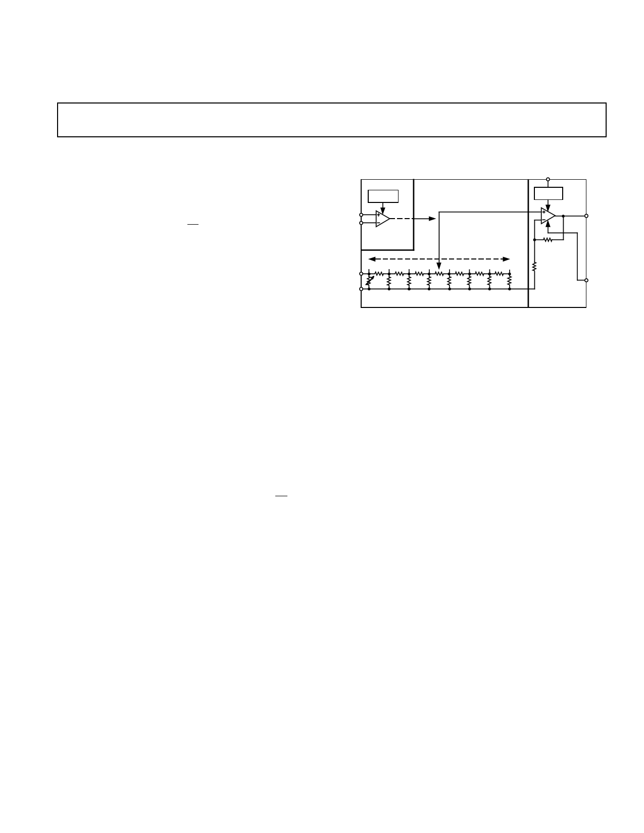
of the “op amp” form of the amplifier, as shown in Figure 1.
The feedback voltage is developed across the resistor RF1
(which, to achieve low noise, has a value of only 20 Ω). The
voltage developed across this resistor is referenced to the input
common, so the output voltage is also referred to that node.
To provide rejection of this common voltage, an auxiliary ampli-
fier (not shown) is included, which senses the voltage difference
between input and output commons and cancels this error
component. Thus, for zero differential signal input between
A1HI and A1LO, the output A1OP simply follows the voltage at
A1CM. Note that the range of voltage differences which can ex-
ist between A1LO and A1CM (or A2LO and A2CM) is limited
to about ± 100 mV. Figure 50 (one of the typical performance
curves at the end of this data sheet) shows typical common-
mode rejection ratio versus frequency.
ACHIEVING 80 dB GAIN RANGE
The two amplifier sections of the X-AMP can be connected in
series to achieve higher gain. In this mode, the output of A1
(A1OP and A1CM) drives the input of A2 via a high-pass
network (usually just a capacitor) that rejects the dc offset. The
nominal gain range is now –2 dB to +82 dB for the AD600 or
–22 dB to +62 dB for the AD602.
There are several options in connecting the gain-control inputs.
The choice depends on the desired signal-to-noise ratio (SNR)
and gain error (output ripple). The following examples feature
the AD600; the arguments generally apply to the AD602, with
appropriate changes to the gain values.
Sequential Mode (Maximum S/N Ratio)
In the sequential mode of operation, the SNR is maintained at
its highest level for as much of the gain control range possible,
as shown in Figure 2. Note here that the gain range is 0 dB to
80 dB. Figure 3 shows the general connections to accomplish
this. Both gain-control inputs, C1HI and C2HI, are driven in
parallel by a positive only, ground referenced source with a
range of 0 V to +2.5 V.
85
80
75
70
65
60
55
50
45
40
35
30
–0.5 0.0 0.5 1.0 1.5 2.0 2.5 3.0
VG
Figure 2. S/N Ratio vs. Control Voltage Sequential Control
(1 MHz Bandwidth)
REV. A
–5–
5 Page 
The emitter circuit of Q1 is somewhat inductive (due its finite ft
and base resistance). Consequently, the effective value of R2 in-
creases with frequency. This would result in an increase in the
stabilized output amplitude at high frequencies, but for the ad-
dition of C3, determined experimentally to be 15 pF for the
2N3904 for maximum response flatness. Alternatively, a faster
transistor can be used here to reduce HF peaking. Figure 16
shows the ac response at the stabilized output level of about
1.3 V rms. Figure 17 demonstrates the output stabilization for
sine wave inputs of 1 mV to 1 V rms at frequencies of 100 kHz,
1 MHz and 10 MHz
AD600/AD602
+5V
AD590
TO AD600 PIN 16
C2
1µF
300µA
(at 300K)
Q1
2N3904
C3
15pF
TO AD600 PIN 11
R2B
R2A VPTAT R2 = R2A R2B ≈ 806Ω
RF
OUTPUT
3dB
0.1 1
10 100
FREQUENCY – MHz
Figure 16. AC Response at the Stabilized Output Level
of 1.3 V RMS
+0.2
0
–0.2
–0.4
100kHz
1MHz
10MHz
0.001
0.01 0.1
INPUT AMPLITUDE – Volts RMS
1
Figure 17. Output Stabilization vs. RMS Input for
Sine Wave Inputs at 100 kHz, 1 MHz, and 10 MHz
While the “bandgap” principle used here sets the output ampli-
tude to 1.2 V (for the square wave case), the stabilization point
can be set to any higher amplitude, up to the maximum output
of ± (VS – 2) V which the AD600 can support. It is only neces-
sary to split R2 into two components of appropriate ratio whose
parallel sum remains close to the zero-TC value of 806 Ω. This
is illustrated in Figure 18, which shows how the output can be
raised, without altering the temperature stability.
Figure 18. Modification in Detector to Raise Output to
2 V RMS
A Wide Range, RMS-Linear dB Measurement System
(2 MHz AGC Amplifier with RMS Detector)
Monolithic rms-dc converters provide an inexpensive means to
measure the rms value of a signal of arbitrary waveform, and
they also may provide a low accuracy logarithmic (“decibel-
scaled”) output. However, they have certain shortcomings. The
first of these is their restricted dynamic range, typically only
50 dB. More troublesome is that the bandwidth is roughly pro-
portional to the signal level; for example, the AD636 provides a
3 dB bandwidth of 900 kHz for an input of 100 mV rms, but
has a bandwidth of only 100 kHz for a 10 mV rms input. Its
logarithmic output is unbuffered, uncalibrated and not stable
over temperature; considerable support circuitry, including at
least two adjustments and a special high TC resistor, is required
to provide a useful output.
All of these problems can be eliminated using an AD636 as
merely the detector element in an AGC loop, in which the differ-
ence between the rms output of the amplifier and a fixed dc ref-
erence are nulled in a loop integrator. The dynamic range and
the accuracy with which the signal can be determined are now
entirely dependent on the amplifier used in the AGC system.
Since the input to the rms-dc converter is forced to a constant
amplitude, close to its maximum input capability, the band-
width is no longer signal dependent. If the amplifier has an ex-
actly exponential (“linear-dB”) gain-control law, its control
voltage VG is forced by the AGC loop to be have the general
form:
VOUT
= VSCALE
log
10
VIN (RMS
VREF
)
(4)
Figure 19 shows a practical wide dynamic range rms-responding
measurement system using the AD600. Note that the signal out-
put of this system is available at A2OP, and the circuit can be
used as a wideband AGC amplifier with an rms-responding de-
tector. This circuit can handle inputs from 100 µV to 1 V rms
with a constant measurement bandwidth of 20 Hz to 2 MHz,
limited primarily by the AD636 rms converter. Its logarithmic
output is a loadable voltage, accurately calibrated to 100 mV/dB,
or 2 V per decade, which simplifies the interpretation of the
reading when using a DVM, and is arranged to be –4 V for an
input of 100 µV rms input, zero for 10 mV, and +4 V for a
1 V rms input. In terms of Equation 4, VREF is 10 mV and
VSCALE is 2 V.
REV. A
–11–
11 Page | ||
| Páginas | Total 20 Páginas | |
| PDF Descargar | [ Datasheet AD600.PDF ] | |
Hoja de datos destacado
| Número de pieza | Descripción | Fabricantes |
| AD600 | Dual/ Low Noise/ Wideband Variable Gain Amplifiers | Analog Devices |
| AD602 | Dual/ Low Noise/ Wideband Variable Gain Amplifiers | Analog Devices |
| AD6025GP | Fan | ADDA |
| AD603 | Variable Gain Amplifier | Analog Devices |
| Número de pieza | Descripción | Fabricantes |
| SLA6805M | High Voltage 3 phase Motor Driver IC. |
Sanken |
| SDC1742 | 12- and 14-Bit Hybrid Synchro / Resolver-to-Digital Converters. |
Analog Devices |
|
DataSheet.es es una pagina web que funciona como un repositorio de manuales o hoja de datos de muchos de los productos más populares, |
| DataSheet.es | 2020 | Privacy Policy | Contacto | Buscar |