|
|
|
PDF AD802 Data sheet ( Hoja de datos )
| Número de pieza | AD802 | |
| Descripción | Clock Recovery and Data Retiming Phase-Locked Loop | |
| Fabricantes | Analog Devices | |
| Logotipo | ||
Hay una vista previa y un enlace de descarga de AD802 (archivo pdf) en la parte inferior de esta página. Total 12 Páginas | ||
|
No Preview Available !
a
Clock Recovery and Data Retiming
Phase-Locked Loop
FEATURES
Standard Products
44.736 Mbps—DS-3
51.84 Mbps—STS-1
155.52 Mbps—STS-3 or STM-1
Accepts NRZ Data, No Preamble Required
Recovered Clock and Retimed Data Outputs
Phase-Locked Loop Type Clock Recovery—No Crystal
Required
Random Jitter: 20؇ Peak-to-Peak
Pattern Jitter: Virtually Eliminated
10KH ECL Compatible
Single Supply Operation: –5.2 V or +5 V
Wide Operating Temperature Range: –40؇C to +85؇C
AD800/AD802*
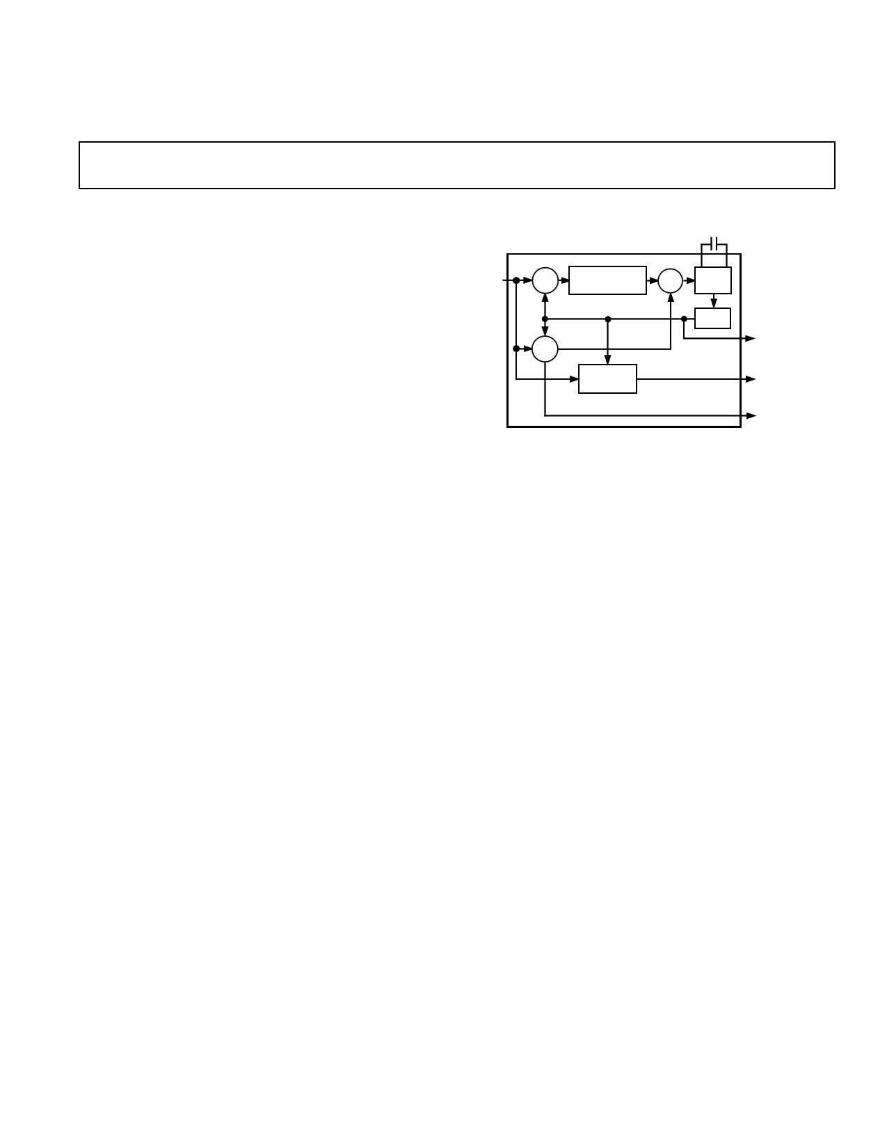
FUNCTIONAL BLOCK DIAGRAM
CD
DATA
INPUT
ØDET
COMPENSATING
ZERO
∑
LOOP
FILTER
VCO
fDET
RETIMING
DEVICE
AD800/AD802
RECOVERED
CLOCK
OUTPUT
RETIMED
DATA
OUTPUT
FRAC
OUTPUT
PRODUCT DESCRIPTION
The AD800 and AD802 employ a second order phase-locked
loop architecture to perform clock recovery and data retiming
on Non-Return to Zero, NRZ, data. This architecture is
capable of supporting data rates between 20 Mbps and 160
Mbps. The products described here have been defined to work
with standard telecommunications bit rates. 45 Mbps DS-3 and
52 Mbps STS-1 are supported by the AD800-45 and
AD800-52 respectively. 155 Mbps STS-3 or STM-1 are
supported by the AD802-155.
Unlike other PLL-based clock recovery circuits, these devices
do not require a preamble or an external VCXO to lock onto
input data. The circuit acquires frequency and phase lock using
two control loops. The frequency acquisition control loop
initially acquires the clock frequency of the input data. The
phase-lock loop then acquires the phase of the input data, and
ensures that the phase of the output signals track changes in the
phase of the input data. The loop damping of the circuit is
dependent on the value of a user selected capacitor; this defines
jitter peaking performance and impacts acquisition time. The
devices exhibit 0.08 dB jitter peaking, and acquire lock on
random or scrambled data within 4 × 105 bit periods when
using a damping factor of 5.
During the process of acquisition the frequency detector
provides a Frequency Acquisition (FRAC) signal which
indicates that the device has not yet locked onto the input data.
This signal is a series of pulses which occur at the points of cycle
slip between the input data and the synthesized clock signal.
Once the circuit has acquired frequency lock no pulses occur at
the FRAC output.
The inclusion of a precisely trimmed VCO in the device
eliminates the need for external components for setting center
frequency, and the need for trimming of those components. The
VCO provides a clock output within ± 20% of the device center
frequency in the absence of input data.
The AD800 and AD802 exhibit virtually no pattern jitter, due
to the performance of the patented phase detector. Total loop
jitter is 20° peak-to-peak. Jitter bandwidth is dictated by mask
programmable fractional loop bandwidth. The AD800, used for
data rates < 90 Mbps, has been designed with a nominal loop
bandwidth of 0.1% of the center frequency. The AD802, used
for data rates in excess of 90 Mbps, has a loop bandwidth of
0.08% of center frequency.
All of the devices operate with a single +5 V or –5.2 V supply.
*Protected by U.S. Patent No. 5,027,085.
REV. B
Information furnished by Analog Devices is believed to be accurate and
reliable. However, no responsibility is assumed by Analog Devices for its
use, nor for any infringements of patents or other rights of third parties
which may result from its use. No license is granted by implication or
otherwise under any patent or patent rights of Analog Devices.
One Technology Way, P.O. Box 9106, Norwood, MA 02062-9106, U.S.A.
Tel: 617/329-4700
Fax: 617/326-8703
1 page 
52
50
48
46
44
42
40
38
–40
–20
0
20 40 60 80 100
TEMPERATURE – °C
Figure 3. AD800-45 Center Frequency vs. Temperature
Typical Characteristics–AD800/AD802
10
9
8
7
6
5
4
3
2
1
0
–40
–20
0 20 40 60
TEMPERATURE – °C
80 100
Figure 4. AD800-45 Jitter vs. Temperature
52
50
48
46
44
42
40
38
–40
–20
0
20 40 60 80 100
TEMPERATURE – °C
Figure 5. AD800-45 Capture and Tracking Range vs.
Temperature
100
AD800-45
10
DS-3 MASK
1
0.1
100
101 102 103 104
JITTER FREQUENCY – Hz
105
Figure 6. AD800-45 Jitter Tolerance
106
55
CD = 0.68µF
53
51
49
47
45
43
41
39
37
35
0
0.05 0.10 0.15 0.20 0.25 0.30
INPUT JITTER – UI p-p
Figure 7. AD800-45 Acquisition Range vs. Input Jitter
1E-1
5E-2
3E-2
2E-2
1E-2
1E-3
1E-4
1E-5
1E-7
1E-9
1E-11
20
80
1 erfc 1 S
2 22 N
80
ECL
20
10 12 14 16 18 20 22 24
S/N – dB
Figure 8. AD800-45 Bit Error Rate vs. Input Jitter
REV. B
–5–
5 Page 
AD800/AD802
Figure 27. Negative Supply Configuration: Component
Side (Top Layer)
Figure 29. Positive Supply Configuration: Component
Side (Top Layer)
Figure 28. Negative Supply Configuration: Solder Side
Figure 30. Positive Supply Configuration: Solder Side
REV. B
–11–
11 Page | ||
| Páginas | Total 12 Páginas | |
| PDF Descargar | [ Datasheet AD802.PDF ] | |
Hoja de datos destacado
| Número de pieza | Descripción | Fabricantes |
| AD800 | Clock Recovery and Data Retiming Phase-Locked Loop | Analog Devices |
| AD8000 | Ultrahigh Speed Op Amp | Analog Devices |
| AD8001 | Current Feedback Amplifier | Analog Devices |
| AD8002 | Dual 600 MHz/ 50 mW Current Feedback Amplifier | Analog Devices |
| Número de pieza | Descripción | Fabricantes |
| SLA6805M | High Voltage 3 phase Motor Driver IC. |
Sanken |
| SDC1742 | 12- and 14-Bit Hybrid Synchro / Resolver-to-Digital Converters. |
Analog Devices |
|
DataSheet.es es una pagina web que funciona como un repositorio de manuales o hoja de datos de muchos de los productos más populares, |
| DataSheet.es | 2020 | Privacy Policy | Contacto | Buscar |