|
|
|
PDF AD7665 Data sheet ( Hoja de datos )
| Número de pieza | AD7665 | |
| Descripción | 16-Bit/ 570 kSPS CMOS ADC | |
| Fabricantes | Analog Devices | |
| Logotipo | ||
1. AD7665 Hay una vista previa y un enlace de descarga de AD7665 (archivo pdf) en la parte inferior de esta página. Total 24 Páginas | ||
|
No Preview Available !
a
16-Bit, 570 kSPS CMOS ADC
FEATURES
Throughput:
570 kSPS (Warp Mode)
500 kSPS (Normal Mode)
INL: ؎2.5 LSB Max (؎0.0038% of Full Scale)
16-Bit Resolution with No Missing Codes
S/(N+D): 90 dB Typ @ 180 kHz
THD: –100 dB Typ @ 180 kHz
Analog Input Voltage Ranges:
Bipolar: ؎10 V, ؎5 V, ؎2.5 V
Unipolar: 0 V to 10 V, 0 V to 5 V, 0 V to 2.5 V
Both AC and DC Specifications
No Pipeline Delay
Parallel (8/16 Bits) and Serial 5 V/3 V Interface
Single 5 V Supply Operation
Power Dissipation
64 mW Typical
15 W @ 100 SPS
Power-Down Mode: 7 W Max
Package: 48-Lead Quad Flatpack (LQFP)
Pin-to-Pin Compatible Upgrade of the AD7664/AD7663
APPLICATIONS
Data Acquisition
Communication
Instrumentation
Spectrum Analysis
Medical Instruments
Process Control
AD7665*
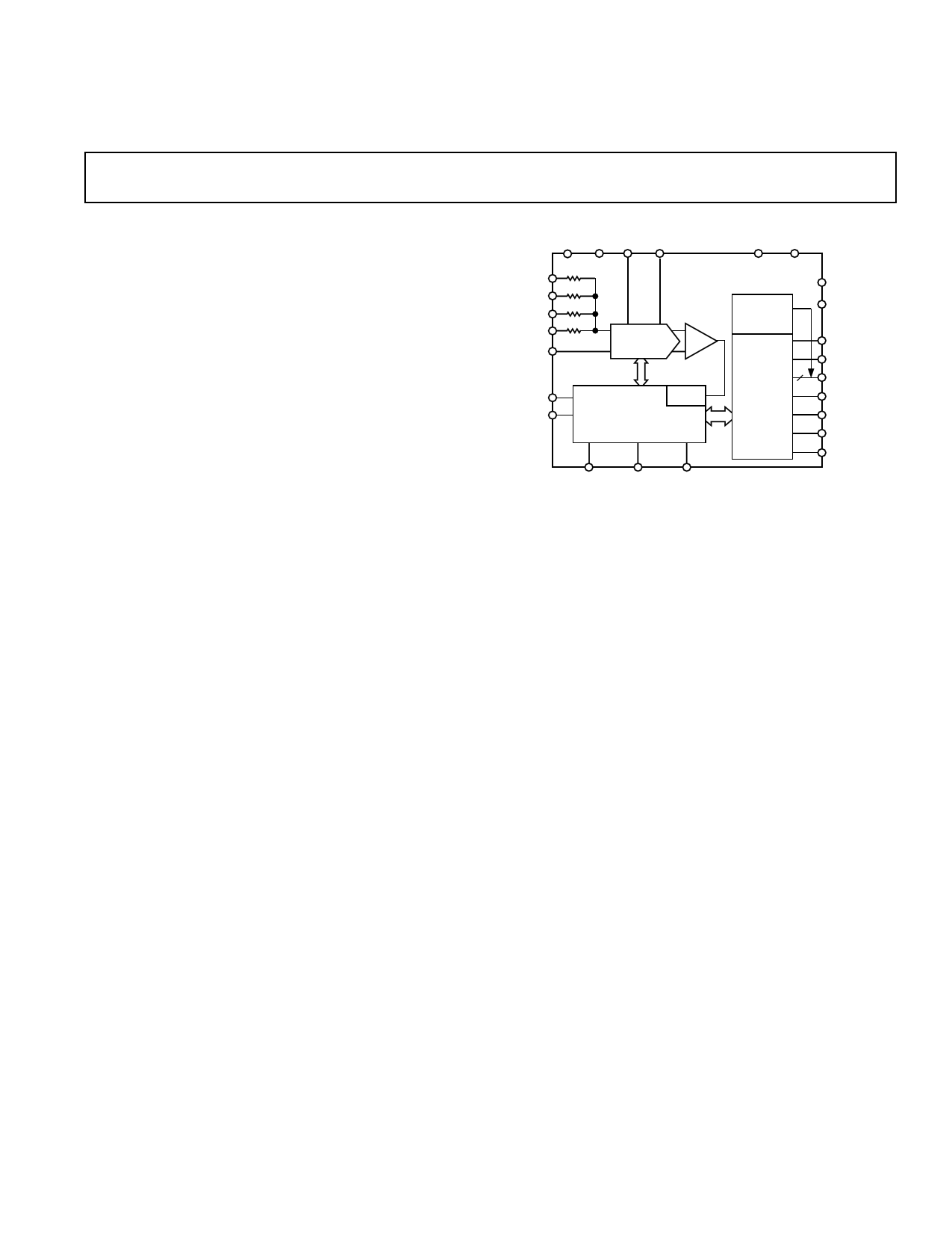
FUNCTIONAL BLOCK DIAGRAM
AVDD AGND REF REFGND
DVDD DGND
IND(4R)
INC(4R)
INB(2R)
INA(R)
INGND
PD
RESET
4R
AD7665
4R
2R
R
SWITCHED
CAP DAC
SERIAL
PORT
CLOCK
PARALLEL 16
INTERFACE
CONTROL LOGIC AND
CALIBRATION CIRCUITRY
WARP IMPULSE CNVST
OVDD
OGND
SER/PAR
BUSY
DATA[15:0]
CS
RD
OB/2C
BYTESWAP
GENERAL DESCRIPTION
The AD7665 is a 16-bit, 570 kSPS, charge redistribution SAR,
analog-to-digital converter that operates from a single 5 V power
supply. It contains a high-speed 16-bit sampling ADC, a resistor
input scaler which allows various input ranges, an internal con-
version clock, error correction circuits, and both serial and
parallel system interface ports.
The AD7665 is hardware factory-calibrated and is comprehen-
sively tested to ensure such ac parameters as signal-to-noise ratio
(SNR) and total harmonic distortion (THD), in addition to the
more traditional dc parameters of gain, offset, and linearity.
It features a very high sampling rate mode (Warp) and, for
asynchronous conversion rate applications, a fast mode (Nor-
mal) and, for low power applications, a reduced power mode
(Impulse) where the power is scaled with the throughput. It is
fabricated using Analog Devices’ high-performance, 0.6 micron
CMOS process and is available in a 48-lead LQFP with opera-
tion specified from –40°C to +85°C.
PRODUCT HIGHLIGHTS
1. Fast Throughput
The AD7665 is a very high speed (570 kSPS in Warp mode
and 500 kSPS in Normal mode), charge redistribution,
16-bit SAR ADC.
2. Single Supply Operation
The AD7665 operates from a single 5 V supply, dissipates
only 64 mW typical, even lower when a reduced throughput
is used with the reduced power mode (Impulse) and a power-
down mode.
3. Superior INL
The AD7665 has a maximum integral nonlinearity of 2.5 LSB
with no missing 16-bit code.
4. Serial or Parallel Interface
Versatile parallel (8 or 16 bits) or 2-wire serial interface
arrangement compatible with both 3 V or 5 V logic.
*Patent pending.
REV. 0
Information furnished by Analog Devices is believed to be accurate and
reliable. However, no responsibility is assumed by Analog Devices for its
use, nor for any infringements of patents or other rights of third parties that
may result from its use. No license is granted by implication or otherwise
under any patent or patent rights of Analog Devices.
One Technology Way, P.O. Box 9106, Norwood, MA 02062-9106, U.S.A.
Tel: 781/329-4700
www.analog.com
Fax: 781/326-8703
© Analog Devices, Inc., 2001
1 page 
1.6mA IOL
TO OUTPUT
PIN
CL
60pF1
500A IOH
1.4V
NOTE:
1IN SERIAL INTERFACE MODES, THE SYNC, SCLK, AND
SDOUT TIMINGS ARE DEFINED WITH A MAXIMUM LOAD
CL OF 10pF; OTHERWISE, THE LOAD IS 60pF MAXIMUM.
Figure 1. Load Circuit for Digital Interface Timing, SDOUT,
SYNC, SCLK Outputs, CL = 10 pF
0.8V
tDELAY
2V
0.8V
2V
tDELAY
2V
0.8V
Figure 2. Voltage Reference Levels for Timing
AD7665
PIN CONFIGURATION
48-Lead LQFP
(ST-48)
48 47 46 45 44 43 42 41 40 39 38 37
AGND 1
AVDD 2
NC 3
BYTESWAP 4
OB/2C 5
WARP 6
IMPULSE 7
SER/PAR 8
D0 9
D1 10
D2/DIVSCLK[0] 11
D3/DIVSCLK[1] 12
PIN 1
IDENTIFIER
AD7665
TOP VIEW
(Not to Scale)
36 AGND
35 CNVST
34 PD
33 RESET
32 CS
31 RD
30 DGND
29 BUSY
28 D15
27 D14
26 D13
25 D12
NC = NO CONNECT
13 14 15 16 17 18 19 20 21 22 23 24
ABSOLUTE MAXIMUM RATINGS1
Analog Inputs
IND2, INC2, INB2 . . . . . . . . . . . . . . . . . . . –11 V to +30 V
INA, REF, INGND, REFGND
. . . . . . . . . . . . . . . . . . . . AGND – 0.3 V to AVDD + 0.3 V
Ground Voltage Differences
AGND, DGND, OGND . . . . . . . . . . . . . . . . . . . . . ± 0.3 V
Supply Voltages
AVDD, DVDD, OVDD . . . . . . . . . . . . . . . . . . . . . . . . . 7 V
AVDD to DVDD, AVDD to OVDD . . . . . . . . . . . . . ± 7 V
DVDD to OVDD . . . . . . . . . . . . . . . . . . . . . . . . . . . . ± 7 V
Digital Inputs . . . . . . . . . . . . . . . –0.3 V to DVDD + 0.3 V
Internal Power Dissipation3 . . . . . . . . . . . . . . . . . . . 700 mW
Junction Temperature . . . . . . . . . . . . . . . . . . . . . . . . . 150°C
Storage Temperature Range . . . . . . . . . . . . –65°C to +150°C
Lead Temperature Range
(Soldering 10 sec) . . . . . . . . . . . . . . . . . . . . . . . . . . 300°C
NOTES
1Stresses above those listed under Absolute Maximum Ratings may cause perma-
nent damage to the device. This is a stress rating only; functional operation of the
device at these or any other conditions above those indicated in the operational
section of this specification is not implied. Exposure to absolute maximum rating
conditions for extended periods may affect device reliability.
2See Analog Input section.
3Specification is for device in free air: 48-Lead LQFP: θJA = 91°C/W, θJC = 30°C/W.
ORDERING GUIDE
Model
Temperature Range
Package Description
Package Option
AD7665AST
AD7665ASTRL
EVAL-AD7665CB1
EVAL-CONTROL BRD22
–40°C to +85°C
–40°C to +85°C
Quad Flatpack (LQFP)
Quad Flatpack (LQFP)
Evaluation Board
Controller Board
ST-48
ST-48
NOTES
1This board can be used as a stand-alone evaluation board or in conjunction with the EVAL-CONTROL BRD2 for evaluation/demonstration purposes.
2This board allows a PC to control and communicate with all Analog Devices evaluation boards ending in the CB designators.
CAUTION
ESD (electrostatic discharge) sensitive device. Electrostatic charges as high as 4000 V readily
accumulate on the human body and test equipment and can discharge without detection. Although
the AD7665 features proprietary ESD protection circuitry, permanent damage may occur on
devices subjected to high-energy electrostatic discharges. Therefore, proper ESD precautions are
recommended to avoid performance degradation or loss of functionality.
WARNING!
ESD SENSITIVE DEVICE
REV. 0
–5–
5 Page 
50
40
30
20
10
0
0 50 100 150 200
CL – pF
TPC 13. Typical Delay vs. Load Capacitance CL
100000
10000
1000
AVDD, WARP/NORMAL
DVDD, WARP/NORMAL
100
AVDD, IMPULSE
10 DVDD, IMPULSE
1
0.1
0.01
OVDD, ALL MODES
0.001
1
10 100 1000 10000 100000 1000000
SAMPLING RATE – SPS
TPC 14. Operating Currents vs. Sample Rate
AD7665
1000
900
800
700
600
500
400
300
200
100
0
–55
–35 –15
DVDD
OVDD
AVDD
5
25 45
65 85 105
TEMPERATURE – ؇C
TPC 15. Power-Down Operating Currents vs. Temperature
REV. 0
–11–
11 Page | ||
| Páginas | Total 24 Páginas | |
| PDF Descargar | [ Datasheet AD7665.PDF ] | |
Hoja de datos destacado
| Número de pieza | Descripción | Fabricantes |
| AD766 | 16-Bit DSP DACPORT | Analog Devices |
| AD7660 | 16-Bit/ 100 kSPS CMOS ADC | Analog Devices |
| AD7661 | 16-Bit 1 MSPS SAR Unipolar ADC with Ref | Analog Devices |
| AD7663 | 250 kSPS CMOS ADC | Analog Devices |
| Número de pieza | Descripción | Fabricantes |
| SLA6805M | High Voltage 3 phase Motor Driver IC. |
Sanken |
| SDC1742 | 12- and 14-Bit Hybrid Synchro / Resolver-to-Digital Converters. |
Analog Devices |
|
DataSheet.es es una pagina web que funciona como un repositorio de manuales o hoja de datos de muchos de los productos más populares, |
| DataSheet.es | 2020 | Privacy Policy | Contacto | Buscar |