|
|
|
PDF AD7664 Data sheet ( Hoja de datos )
| Número de pieza | AD7664 | |
| Descripción | 16-Bit/ 570 kSPS CMOS ADC | |
| Fabricantes | Analog Devices | |
| Logotipo | ||
Hay una vista previa y un enlace de descarga de AD7664 (archivo pdf) en la parte inferior de esta página. Total 19 Páginas | ||
|
No Preview Available !
a
FEATURES
Throughput:
570 kSPS (Warp Mode)
500 kSPS (Normal Mode)
INL: ؎2.5 LSB Max (؎0.0038% of Full-Scale)
16 Bits Resolution with No Missing Codes
S/(N+D): 90 dB Typ @ 10 kHz
THD: –100 dB Typ @ 10 kHz
Analog Input Voltage Range: 0 V to 2.5 V
Both AC and DC Specifications
No Pipeline Delay
Parallel and Serial 5 V/3 V Interface
Single 5 V Supply Operation
Power Dissipation
97 mW Typical,
21 W @ 100 SPS
Power-Down Mode: 7 W Max
Package: 48-Lead Quad Flat Pack (LQFP)
Pin-to-Pin Compatible Upgrade of the AD7660
APPLICATIONS
Data Acquisition
Instrumentation
Digital Signal Processing
Spectrum Analysis
Medical Instruments
Battery-Powered Systems
Process Control
16-Bit, 570 kSPS CMOS ADC
AD7664*
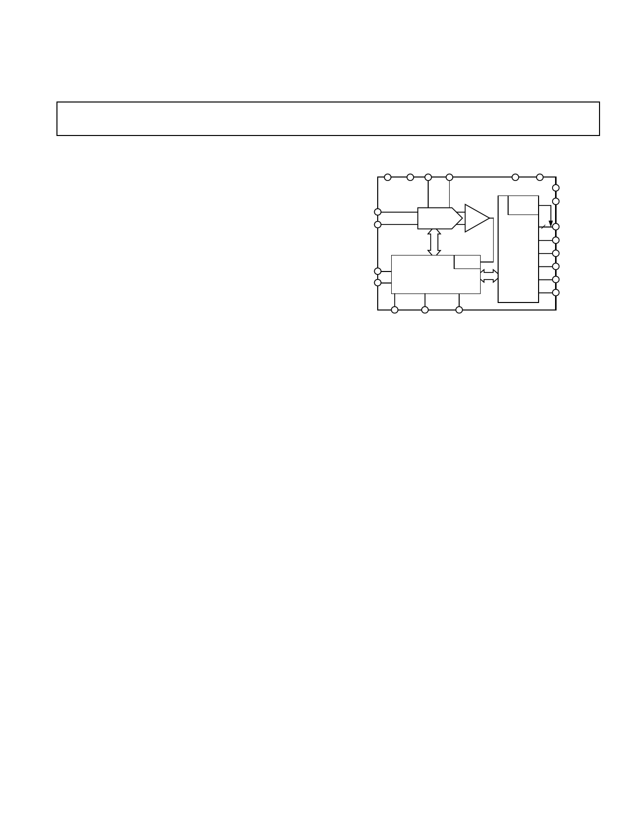
FUNCTIONAL BLOCK DIAGRAM
AVDD AGND REF REFGND
DVDD DGND
IN
INGND
PD
RESET
AD7664
SWITCHED
CAP DAC
SERIAL
PORT
16
CLOCK
CONTROL LOGIC AND
CALIBRATION CIRCUITRY
PARALLEL
INTERFACE
OVDD
OGND
DATA[15:0]
BUSY
RD
CS
SER/PAR
OB/2C
WARP IMPULSE CNVST
GENERAL DESCRIPTION
The AD7664 is a 16-bit, 570 kSPS, charge redistribution SAR,
analog-to-digital converter that operates from a single 5 V power
supply. The part contains a high-speed 16-bit sampling ADC,
an internal conversion clock, error correction circuits, and both
serial and parallel system interface ports.
The AD7664 is hardware factory calibrated and is comprehensively
tested to ensure such ac parameters as signal-to-noise ratio (SNR)
and total harmonic distortion (THD), in addition to the more
traditional dc parameters of gain, offset, and linearity.
It features a very high sampling rate mode (Warp) and, for asyn-
chronous conversion rate applications, a fast mode (Normal)
and, for low power applications, a reduced power mode (Impulse)
where the power is scaled with the throughput.
It is fabricated using Analog Devices’ high-performance, 0.6
micron CMOS process, with correspondingly low cost and is
available in a 48-lead LQFP with operation specified from –40°C
to +85°C.
PRODUCT HIGHLIGHTS
1. Fast Throughput
The AD7664 is a 570 kSPS, charge redistribution, 16-bit
SAR ADC with internal error correction circuitry.
2. Superior INL
The AD7664 has a maximum integral nonlinearity of 2.5 LSBs
with no missing 16-bit code.
3. Single-Supply Operation
The AD7664 operates from a single 5 V supply and typically
dissipates only 97 mW. In impulse mode, its power dissipa-
tion decreases with the throughput to, for instance, only 21 µW
at a 100 SPS throughput. It consumes 7 µW maximum when in
power-down.
4. Serial or Parallel Interface
Versatile parallel or 2-wire serial interface arrangement com-
patible with both 3 V or 5 V logic.
*Patent pending.
REV. 0
Information furnished by Analog Devices is believed to be accurate and
reliable. However, no responsibility is assumed by Analog Devices for its
use, nor for any infringements of patents or other rights of third parties
which may result from its use. No license is granted by implication or
otherwise under any patent or patent rights of Analog Devices.
One Technology Way, P.O. Box 9106, Norwood, MA 02062-9106, U.S.A.
Tel: 781/329-4700 World Wide Web Site: http://www.analog.com
Fax: 781/326-8703
© Analog Devices, Inc., 2000
1 page 
1.6mA IOL
TO OUTPUT
PIN CL
60pF1
500A
IOH
؉1.4V
Figure 1. Load Circuit for Digital Interface Timing,
SDOUT, SYNC, SCLK Outputs, CL = 10 pF
0.8V
tDELAY
2V
0.8V
2V
tDELAY
2V
0.8V
Figure 2. Voltage Reference Levels for Timing
AD7664
PIN CONFIGURATION
48-Lead LQFP
(ST-48)
48 47 46 45 44 43 42 41 40 39 38 37
AGND 1
AVDD 2
NC 3
DGND 4
OB/2C 5
WARP 6
IMPULSE 7
SER/PAR 8
D0 9
D1 10
D2 11
D3 12
PIN 1
IDENTIFIER
AD7664
TOP VIEW
(Not to Scale)
36 AGND
35 CNVST
34 PD
33 RESET
32 CS
31 RD
30 DGND
29 BUSY
28 D15
27 D14
26 D13
25 D12
NC = NO CONNECT
13 14 15 16 17 18 19 20 21 22 23 24
Pin
No.
1
2
3, 40–48
4, 30
5
6
7
8
9–12
13
14
15
Mnemonic
AGND
AVDD
NC
DGND
OB/2C
WARP
IMPULSE
SER/PAR
DATA[0:3]
DATA[4]
or EXT/INT
DATA[5]
or INVSYNC
DATA[6]
or INVSCLK
Type
P
P
DI
DI
DI
DI
DI
DO
DI/O
DI/O
DI/O
PIN FUNCTION DESCRIPTIONS
Description
Analog Power Ground Pin.
Input Analog Power Pins. Nominally 5 V.
No Connect.
Must Be Tied to Analog Ground.
Straight Binary/Binary Two’s Complement. When OB/2C is HIGH, the digital output is
straight binary; when LOW, the MSB is inverted resulting in a two’s complement output
from its internal shift register.
Mode Selection. When HIGH and IMPULSE LOW, this input selects the fastest mode, the
maximum throughput is achievable, and a minimum conversion rate must be applied in order
to guarantee full specified accuracy. When LOW, full accuracy is maintained independent of
the minimum conversion rate.
Mode Selection. When HIGH and WARP LOW, this input selects a reduced power mode. In
this mode, the power dissipation is approximately proportional to the sampling rate.
Serial/Parallel Selection Input. When LOW, the parallel port is selected; when HIGH, the
serial interface mode is selected and some bits of the DATA bus are used as a serial port.
Bit 0 to Bit 3 of the Parallel Port Data Output Bus. These pins are always outputs, regardless
of the state of SER/PAR.
When SER/PAR is LOW, this output is used as Bit 4 of the Parallel Port Data Output Bus.
When SER/PAR is HIGH, this input, part of the serial port, is used as a digital select input
for choosing the internal or an external data clock. With EXT/INT tied LOW, the internal
clock is selected on SCLK output. With EXT/INT set to a logic HIGH, output data is syn-
chronized to an external clock signal connected to the SCLK input.
When SER/PAR is LOW, this output is used as Bit 5 of the Parallel Port Data Output Bus.
When SER/PAR is HIGH, this input, part of the serial port, is used to select the active state
of the SYNC signal. It is active in both master and slave mode. When LOW, SYNC is active
HIGH. When HIGH, SYNC is active LOW.
When SER/PAR is LOW, this output is used as Bit 6 of the Parallel Port Data Output Bus.
When SER/PAR is HIGH, this input, part of the serial port, is used to invert the SCLK sig-
nal. It is active in both master and slave mode.
REV. 0
–5–
5 Page 
AD7664
Table I. Output Codes and Ideal Input Voltages
Description
Analog
Input
Digital Output Code
Hexa
Straight Two’s
Binary Complement
FSR –1 LSB
FSR – 2 LSB
Midscale + 1 LSB
Midscale
Midscale – 1 LSB
–FSR + 1 LSB
–FSR
2.499962 V
2.499923 V
1.250038 V
1.25 V
1.249962 V
38 µV
0V
FFFF1
FFFE
8001
8000
7FFF
0001
00002
7FFF1
7FFE
0001
0000
FFFF
8001
80002
NOTES
1This is also the code for overrange analog input (VIN – VINGND above
VREF – VREFGND).
2This is also the code for underrange analog input (VIN below VINGND)
TYPICAL CONNECTION DIAGRAM
Figure 5 shows a typical connection diagram for the AD7664.
Analog Input
Figure 6 shows an equivalent circuit of the input structure of
the AD7664.
IN
OR INGND
AGND
AVDD
D1
C1
D2
R1 C2
Figure 6. Equivalent Analog Input Circuit
The two diodes D1 and D2 provide ESD protection for the
analog inputs IN and INGND. Care must be taken to ensure
that the analog input signal never exceeds the supply rails by more
than 0.3 V. This will cause these diodes to become forward-
biased and start conducting current. These diodes can handle
a forward-biased current of 100 mA maximum. For instance,
these conditions could eventually occur when the input buffer’s
(U1) supplies are different from AVDD. In such case, an input
buffer with a short circuit current limitation can be used to
protect the part.
ANALOG
SUPPLY
(5V)
10F 100nF
100⍀
10F 100nF
100nF
10F
DIGITAL SUPPLY
(3.3V OR 5V)
AVDD AGND
DGND DVDD OVDD OGND
2.5V REF1
CREF1
REF
100nF
REFGND
ANALOG INPUT
(0V TO 2.5V)
15⍀
U12
IN
CC 2.7nF
INGND
PD
AD7664
RESET
CS
SCLK
SDOUT
BUSY
CNVST
OB/ 2C
SER/ PAR
WARP
IMPULSE
RD
SERIAL
PORT
D3
DVDD
C/ P/DSP
CLOCK
NOTES:
1 THE AD780 IS RECOMMENDED WITH CREF = 47F.
2 THE AD829 IS RECOMMENDED WITH A COMPENSATION CAPACITOR CC = 82 pF, TYPE CERAMIC NPO.
3 OPTIONAL LOW JITTER CNVST.
Figure 5. Typical Connection Diagram
REV. 0
–11–
11 Page | ||
| Páginas | Total 19 Páginas | |
| PDF Descargar | [ Datasheet AD7664.PDF ] | |
Hoja de datos destacado
| Número de pieza | Descripción | Fabricantes |
| AD766 | 16-Bit DSP DACPORT | Analog Devices |
| AD7660 | 16-Bit/ 100 kSPS CMOS ADC | Analog Devices |
| AD7661 | 16-Bit 1 MSPS SAR Unipolar ADC with Ref | Analog Devices |
| AD7663 | 250 kSPS CMOS ADC | Analog Devices |
| Número de pieza | Descripción | Fabricantes |
| SLA6805M | High Voltage 3 phase Motor Driver IC. |
Sanken |
| SDC1742 | 12- and 14-Bit Hybrid Synchro / Resolver-to-Digital Converters. |
Analog Devices |
|
DataSheet.es es una pagina web que funciona como un repositorio de manuales o hoja de datos de muchos de los productos más populares, |
| DataSheet.es | 2020 | Privacy Policy | Contacto | Buscar |