|
|
|
PDF AD974 Data sheet ( Hoja de datos )
| Número de pieza | AD974 | |
| Descripción | 4-Channel/ 16-Bit/ 200 kSPS Data Acquisition System | |
| Fabricantes | Analog Devices | |
| Logotipo | ||
Hay una vista previa y un enlace de descarga de AD974 (archivo pdf) en la parte inferior de esta página. Total 20 Páginas | ||
|
No Preview Available !
a
4-Channel, 16-Bit, 200 kSPS
Data Acquisition System
AD974
FEATURES
Fast 16-Bit ADC with 200 kSPS Throughput
Four Single-Ended Analog Input Channels
Single +5 V Supply Operation
Input Ranges: 0 V to +4 V, 0 V to +5 V and ؎10 V
120 mW Max Power Dissipation
Power-Down Mode 50 W
Choice of External or Internal 2.5 V Reference
On-Chip Clock
Power-Down Mode
GENERAL DESCRIPTION
The AD974 is a four-channel, data acquisition system with a
serial interface. The part contains an input multiplexer, a high-
speed 16-bit sampling ADC and a +2.5 V reference. All of this
operates from a single +5 V power supply that also has a power-
down mode. The part will accommodate 0 V to +4 V, 0 V to
+5 V or ± 10 V analog input ranges.
The interface is designed for an efficient transfer of data while
requiring a low number of interconnects.
The AD974 is comprehensively tested for ac parameters such as
SNR and THD, as well as the more traditional parameters of
offset, gain and linearity.
The AD974 is fabricated on Analog Devices’ BiCMOS process,
which has high performance bipolar devices along with CMOS
transistors.
The AD974 is available in 28-lead DIP, SOIC and SSOP
packages.
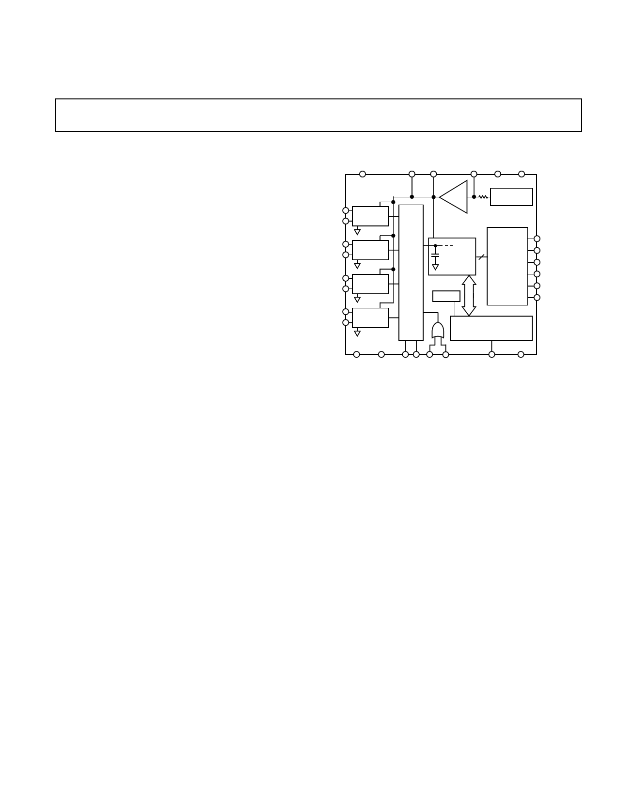
FUNCTIONAL BLOCK DIAGRAM
PWRD
BIP CAP
REF VDIG VANA
V1A
V1B
V2A
V2B
V3A
V3B
V4A
V4B
RESISTIVE
NETWORK
RESISTIVE
NETWORK
RESISTIVE
NETWORK
RESISTIVE
NETWORK
4 TO 1
MUX
+
LATCH
EN
REF
BUFF
2.5V
REFERENCE
AD974
SWITCHED 16
CAP ADC
SERIAL
INTERFACE
CLOCK
EXT/INT
DATACLK
DATA
R/C
CS
SYNC
CONTROL LOGIC
&
CALIBRATION CIRCUITRY
AGND1 AGND2 A0 A1 WR1 WR2
BUSY DGND
PRODUCT HIGHLIGHTS
1. The AD974 is a complete data acquisition system combining
a four-channel multiplexer, a 16-bit sampling ADC and a
+2.5 V reference on a single chip.
2. The part operates from a single +5 V supply and also has a
power-down feature.
3. Interfacing to the AD974 is simple with a low number of
interconnect signals.
4. The AD974 is comprehensively specified for ac parameters
such as SNR and THD, as well as dc parameters such as
linearity and offset and gain errors.
REV. A
Information furnished by Analog Devices is believed to be accurate and
reliable. However, no responsibility is assumed by Analog Devices for its
use, nor for any infringements of patents or other rights of third parties
which may result from its use. No license is granted by implication or
otherwise under any patent or patent rights of Analog Devices.
One Technology Way, P.O. Box 9106, Norwood, MA 02062-9106, U.S.A.
Tel: 781/329-4700 World Wide Web Site: http://www.analog.com
Fax: 781/326-8703
© Analog Devices, Inc., 1999
1 page 
Pin No.
1
2–5, 25–28
6
7
8
Mnemonic
AGND1
VxA, VxB
BIP
CAP
REF
9 AGND2
10 R/C
11 VDIG
12 PWRD
13 EXT/INT
14 DGND
15 SYNC
16 DATACLK
17 DATA
18, 19
20
21
22, 23
WR1, WR2
CS
BUSY
A1, A0
24 VANA
AD974
PIN FUNCTION DESCRIPTIONS
Description
Analog Ground. Used as the ground reference point for the REF pin.
Analog Input. Refer to Table I for input range configuration.
Bipolar Offset. Connect VxA inputs to provide Bipolar input range.
Reference Buffer Output. Connect a 2.2 µF tantalum capacitor between CAP and Analog
Ground.
Reference Input/Output. The internal +2.5 V reference is available at this pin. Alternatively an
external reference can be used to override the internal reference. In either case, connect a 2.2 µF
tantalum capacitor between REF and Analog Ground.
Analog Ground.
Read/Convert Input. Used to control the conversion and read modes. With CS LOW, a falling
edge on R/C holds the analog input signal internally and starts a conversion; a rising edge enables
the transmission of the conversion result.
Digital Power Supply. Nominally +5 V.
Power-Down Input. When set to a logic HIGH, power consumption is reduced and conversions
are inhibited. The conversion result from the previous conversion is stored in the onboard shift
register.
Digital select input for choosing the internal or an external data clock. With EXT/INT tied LOW,
after initiating a conversion, 16 DATACLK pulses transmit the previous conversion result as
shown in Figure 3. With EXT/INT set to a Logic HIGH, output data is synchronized to an
external clock signal connected to the DATACLK input. Data is output as indicated in Figure 4
through Figure 9.
Digital Ground.
Digital output frame synchronization for use with an external data clock (EXT/INT = Logic
HIGH). When a read sequence is initiated, a pulse one DATACLK period wide is output
synchronous to the external data clock.
Serial data clock input or output, dependent upon the logic state of the EXT/INT pin. When
using the internal data clock (EXT/INT = Logic LOW), a conversion start sequence will initiate
transmission of 16 DATACLK periods. Output data is synchronous to this clock and is valid on
both its rising and falling edges (Figure 3). When using an external data clock (EXT/INT = Logic
HIGH), the CS and R/C signals control how conversion data is accessed.
The serial data output is synchronized to DATACLK. Conversion results are stored in an on-
chip register. The AD974 provides the conversion result, MSB first, from its internal shift regis-
ter. When using the internal data clock (EXT/INT = Logic LOW), DATA is valid on both the
rising and falling edges of DATACLK. Using an external data clock (EXT/INT = Logic HIGH)
allows previous conversion data to be accessed during a conversion (Figures 5, 7 and 9) or the
conversion result can be accessed after the completion of a conversion (Figures 4, 6 and 8).
Multiplexer Write Inputs. These inputs are internally ORed to generate the mux latch inputs.
The latch is transparent when WR1 and WR2 are tied low.
Chip Select Input. With R/C LOW, a falling edge on CS will initiate a conversion. With R/C
HIGH, a falling edge on CS will enable the serial data output sequence.
Busy Output. Goes LOW when a conversion is started, and remains LOW until the conversion is
completed and the data is latched into the on-chip shift register.
Address multiplexer inputs latched with the WR1, WR2 inputs.
A1 A0 Data Available from Channel
0 0 AIN 1
0 1 AIN 2
1 0 AIN 3
1 1 AIN 4
Analog Power Supply. Nominally +5 V.
REV. A
–5–
5 Page 
EXTERNAL CONTINUOUS CLOCK DATA READ AFTER
CONVERSION WITH SYNC OUTPUT GENERATED
Figure 8 illustrates the method by which data from conversion
“n” can be read after the conversion is complete using a con-
tinuous external clock, with the generation of a SYNC output.
What permits the generation of a SYNC output is a transition of
DATACLK either while CS is high or while both CS and R/C are
low.
With a continuous clock the CS pin cannot be tied low as it
could be with a discontinuous clock. Use of a continuous clock,
while a conversion is occurring, can increase the DNL and
Transition Noise of the AD974.
After a conversion is complete, indicated by BUSY returning
high, the result of that conversion can be read while CS is low
AD974
and R/C is high. In Figure 8 clock pulse #0 is used to enable the
generation of a SYNC pulse. The SYNC pulse is actually clocked
out approximately 40 ns after the rising edge of clock pulse #1.
The SYNC pulse will be valid on the falling edge of clock pulse
#1 and the rising edge of clock pulse #2. The MSB will be valid
on the falling edge of clock pulse #2 and the rising edge of clock
pulse #3. The LSB will be valid on the falling edge of clock
pulse #17 and the rising edge of clock pulse #18.
When reading data after the conversion is complete, with the
highest frequency permitted for DATACLK (15.15 MHz) the
maximum possible throughput is approximately 195 kHz and
not the rated 200 kHz.
EXT
DATACLK
CS
R/C
BUSY
SYNC
DATA
t12
t13 t14
01 234
t1 t15
t10
t2
t16
t17
t12
t18
BIT 15
(MSB)
BIT 14
17 18
t19
BIT 0
(LSB)
t18
Figure 8. Conversion and Read Timing Using an External Continuous Data Clock (EXT/ INT Set to Logic High)
REV. A
–11–
11 Page | ||
| Páginas | Total 20 Páginas | |
| PDF Descargar | [ Datasheet AD974.PDF ] | |
Hoja de datos destacado
| Número de pieza | Descripción | Fabricantes |
| AD9700 | Video Dispaly D/A Converter | ETC |
| AD9700 | Monolithic Video D/A Converter | Analog Devices |
| AD9701 | 250 MSPS Video Digital-to-Analog Converter | Analog Devices |
| AD9702 | Triple 4-Bit D/A Converter | Analog Devices |
| Número de pieza | Descripción | Fabricantes |
| SLA6805M | High Voltage 3 phase Motor Driver IC. |
Sanken |
| SDC1742 | 12- and 14-Bit Hybrid Synchro / Resolver-to-Digital Converters. |
Analog Devices |
|
DataSheet.es es una pagina web que funciona como un repositorio de manuales o hoja de datos de muchos de los productos más populares, |
| DataSheet.es | 2020 | Privacy Policy | Contacto | Buscar |