|
|
|
PDF AD9201 Data sheet ( Hoja de datos )
| Número de pieza | AD9201 | |
| Descripción | Dual Channel/ 20 MHz 10-Bit Resolution CMOS ADC | |
| Fabricantes | Analog Devices | |
| Logotipo | ||
Hay una vista previa y un enlace de descarga de AD9201 (archivo pdf) en la parte inferior de esta página. Total 20 Páginas | ||
|
No Preview Available !
a
FEATURES
Complete Dual Matching ADCs
Low Power Dissipation: 215 mW (+3 V Supply)
Single Supply: 2.7 V to 5.5 V
Differential Nonlinearity Error: 0.4 LSB
On-Chip Analog Input Buffers
On-Chip Reference
Signal-to-Noise Ratio: 57.8 dB
Over Nine Effective Bits
Spurious-Free Dynamic Range: –73 dB
No Missing Codes Guaranteed
28-Lead SSOP
Dual Channel, 20 MHz 10-Bit
Resolution CMOS ADC
AD9201
IINA
IINB
IREFB
IREFT
QREFB
QREFT
VREF
REFSENSE
QINB
QINA
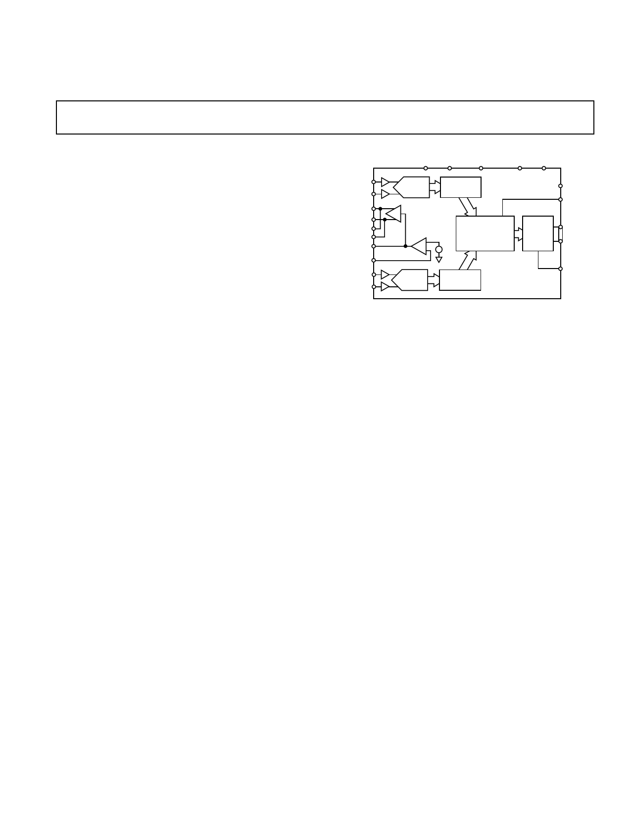
FUNCTIONAL BLOCK DIAGRAM
AVDD AVSS CLOCK
DVDD DVSS
"I" ADC
I
REGISTER
AD9201
REFERENCE
BUFFER
ASYNCHRONOUS
MULTIPLEXER
1V
THREE-
STATE
OUTPUT
BUFFER
"Q" ADC
Q
REGISTER
SLEEP
SELECT
DATA
10 BITS
CHIP
SELECT
PRODUCT DESCRIPTION
The AD9201 is a complete dual channel, 20 MSPS, 10-bit
CMOS ADC. The AD9201 is optimized specifically for applica-
tions where close matching between two ADCs is required (e.g.,
I/Q channels in communications applications). The 20 MHz
sampling rate and wide input bandwidth will cover both narrow-
band and spread-spectrum channels. The AD9201 integrates two
10-bit, 20 MSPS ADCs, two input buffer amplifiers, an internal
voltage reference and multiplexed digital output buffers.
Each ADC incorporates a simultaneous sampling sample-and-
hold amplifier at its input. The analog inputs are buffered; no
external input buffer op amp will be required in most applica-
tions. The ADCs are implemented using a multistage pipeline
architecture that offers accurate performance and guarantees no
missing codes. The outputs of the ADCs are ported to a multi-
plexed digital output buffer.
The AD9201 is manufactured on an advanced low cost CMOS
process, operates from a single supply from 2.7 V to 5.5 V, and
consumes 215 mW of power (on 3 V supply). The AD9201 input
structure accepts either single-ended or differential signals,
providing excellent dynamic performance up to and beyond
its 10 MHz Nyquist input frequencies.
PRODUCT HIGHLIGHTS
1. Dual 10-Bit, 20 MSPS ADCs
A pair of high performance 20 MSPS ADCs that are opti-
mized for spurious free dynamic performance are provided for
encoding of I and Q or diversity channel information.
2. Low Power
Complete CMOS Dual ADC function consumes a low
215 mW on a single supply (on 3 V supply). The AD9201
operates on supply voltages from 2.7 V to 5.5 V.
3. On-Chip Voltage Reference
The AD9201 includes an on-chip compensated bandgap
voltage reference pin programmable for 1 V or 2 V.
4. On-chip analog input buffers eliminate the need for external
op amps in most applications.
5. Single 10-Bit Digital Output Bus
The AD9201 ADC outputs are interleaved onto a single
output bus saving board space and digital pin count.
6. Small Package
The AD9201 offers the complete integrated function in a
compact 28-lead SSOP package.
7. Product Family
The AD9201 dual ADC is pin compatible with a dual 8-bit
ADC (AD9281) and has a companion dual DAC product,
the AD9761 dual DAC.
REV. D
Information furnished by Analog Devices is believed to be accurate and
reliable. However, no responsibility is assumed by Analog Devices for its
use, nor for any infringements of patents or other rights of third parties
which may result from its use. No license is granted by implication or
otherwise under any patent or patent rights of Analog Devices.
One Technology Way, P.O. Box 9106, Norwood, MA 02062-9106, U.S.A.
Tel: 781/329-4700 World Wide Web Site: http://www.analog.com
Fax: 781/326-8703
© Analog Devices, Inc., 1999
1 page 
AVDD
DRVDD
AVDD
AVDD
AD9201
AVDD
AVDD
DRVSS
DRVSS
AVSS
a. D0–D9, OTR
AVSS
AVSS
b. Three-State, Standby
AVSS
AVSS
c. CLK
AVDD
IN
AVDD
AVSS
AVSS
d. INA, INB
AVDD
AVDD
REFBS
AVSS
AVDD
REFBF
AVSS
AVSS
e. Reference
f. REFSENSE
Figure 2. Equivalent Circuits
AVDD
AVSS
g. VREF
OFFSET ERROR
The first transition should occur at a level 1 LSB above “zero.”
Offset is defined as the deviation of the actual first code transi-
tion from that point.
OFFSET MATCH
The change in offset error between I and Q channels.
EFFECTIVE NUMBER OF BITS (ENOB)
For a sine wave, SINAD can be expressed in terms of the num-
ber of bits. Using the following formula,
N = (SINAD – 1.76)/6.02
It is possible to get a measure of performance expressed as N,
the effective number of bits.
Thus, effective number of bits for a device for sine wave inputs
at a given input frequency can be calculated directly from its
measured SINAD.
TOTAL HARMONIC DISTORTION (THD)
THD is the ratio of the rms sum of the first six harmonic com-
ponents to the rms value of the measured input signal and
is expressed as a percentage or in decibels.
SIGNAL-TO-NOISE RATIO (SNR)
SNR is the ratio of the rms value of the measured input signal to
the rms sum of all other spectral components below the Nyquist
frequency, excluding the first six harmonics and dc. The value
for SNR is expressed in decibels.
scale. Gain error is the deviation of the actual difference be-
tween first and last code transitions and the ideal difference
between the first and last code transitions.
GAIN MATCH
The change in gain error between I and Q channels.
PIPELINE DELAY (LATENCY)
The number of clock cycles between conversion initiation and
the associated output data being made available. New output
data is provided every rising clock edge.
MUX SELECT DELAY
The delay between the change in SELECT pin data level and
valid data on output pins.
POWER SUPPLY REJECTION
The specification shows the maximum change in full scale from
the value with the supply at the minimum limit to the value with
the supply at its maximum limit.
APERTURE JITTER
Aperture jitter is the variation in aperture delay for successive
samples and is manifested as noise on the input to the A/D.
APERTURE DELAY
Aperture delay is a measure of the Sample-and-Hold Amplifier
(SHA) performance and is measured from the rising edge of the
clock input to when the input signal is held for conversion.
SPURIOUS FREE DYNAMIC RANGE (SFDR)
The difference in dB between the rms amplitude of the input
signal and the peak spurious signal.
GAIN ERROR
The first code transition should occur for an analog value 1 LSB
above nominal negative full scale. The last transition should
occur for an analog value 1 LSB below the nominal positive full
SIGNAL-TO-NOISE AND DISTORTION (S/N+D, SINAD)
RATIO
S/N+D is the ratio of the rms value of the measured input signal
to the rms sum of all other spectral components below the
Nyquist frequency, including harmonics but excluding dc.
The value for S/N+D is expressed in decibels.
REV. D
–5–
5 Page 
0.1F
IREFT
10F 0.1F
0.1F
IREFB
10F
VREF
0.1F
REFSENSE
10k⍀
ADC
CORE
1V
QREFT
0.1F
0.1F
10F
QREFB
0.1F
AVSS
10k⍀
INTERNAL
CONTROL
LOGIC
AD9201
Figure 26. Reference Buffer Equivalent Circuit and Exter-
nal Decoupling Recommendation
For best results in both noise suppression and robustness
against crosstalk, the 4 capacitor buffer decoupling arrangement
shown in Figure 26 is recommended. This decoupling should
feature chip capacitors located close to the converter IC. The
capacitors are connected to either IREFT/IREFB or QREFT/
QREFB. A connection to both sides is not required.
DRIVING THE AD9201
Figure 27 illustrates the use of an AD8051 to drive the AD9201.
Even though the AD8051 is specified with 3 V and 5 V power,
the best results are obtained at ± 5 V power. The ADC input
span is 2 V.
AD9201
VREF
22⍀
AD8051
1k⍀
10pF 17
ADC
3
6 24⍀ 0.33F
22⍀
16
50⍀
2
1k⍀
10pF
1k⍀
0.01F
Figure 27.
10 FUND
0
–10
–20
–30
–40
–50
2ND
–60
3RD
–70 4TH 6TH
–80 8TH
7TH 5TH
–90
–100
–110
–120
0.0E+0
2.0E+6
4.0E+6
6.0E+6
8.0E+6
10.0E+6
1.0E+6
3.0E+6
5.0E+6
7.0E+6
9.0E+6
Figure 28. AD8051/AD9201 Performance
REV. D
–11–
11 Page | ||
| Páginas | Total 20 Páginas | |
| PDF Descargar | [ Datasheet AD9201.PDF ] | |
Hoja de datos destacado
| Número de pieza | Descripción | Fabricantes |
| AD9200 | CMOS A/D Converter | Analog Devices |
| AD9201 | Dual Channel/ 20 MHz 10-Bit Resolution CMOS ADC | Analog Devices |
| AD9203 | A/D Converter | Analog Devices |
| AD9204 | 1.8V Dual Analog-to-Digital Converter | Analog Devices |
| Número de pieza | Descripción | Fabricantes |
| SLA6805M | High Voltage 3 phase Motor Driver IC. |
Sanken |
| SDC1742 | 12- and 14-Bit Hybrid Synchro / Resolver-to-Digital Converters. |
Analog Devices |
|
DataSheet.es es una pagina web que funciona como un repositorio de manuales o hoja de datos de muchos de los productos más populares, |
| DataSheet.es | 2020 | Privacy Policy | Contacto | Buscar |