|
|
|
PDF AD8348 Data sheet ( Hoja de datos )
| Número de pieza | AD8348 | |
| Descripción | 50-1000 MHz Quadrature Demodulator | |
| Fabricantes | Analog Devices | |
| Logotipo | ||
1. AD8348 Hay una vista previa y un enlace de descarga de AD8348 (archivo pdf) en la parte inferior de esta página. Total 29 Páginas | ||
|
No Preview Available !
FEATURES
Integrated I/Q demodulator with IF VGA amplifier
Operating IF frequency 50 MHz to 1000 MHz
(3 dB IF BW of 500 MHz driven from RS = 200 Ω)
Demodulation bandwidth 75 MHz
Linear-in-decibel AGC range 44 dB
Third-order intercept
IIP3 +28 dBm @ minimum gain (FIF = 380 MHz)
IIP3 −8 dBm @ maximum gain (FIF = 380 MHz)
Quadrature demodulation accuracy
Phase accuracy 0.5°
Amplitude balance 0.25 dB
Noise figure 11 dB @ maximum gain (FIF = 380 MHz)
LO input −10 dBm
Single supply 2.7 V to 5.5 V
Power-down mode
Compact, 28-lead TSSOP package
APPLICATIONS
QAM/QPSK demodulator
W-CDMA/CDMA/GSM/NADC
Wireless local loop
LMDS
GENERAL DESCRIPTION
The AD8348 is a broadband quadrature demodulator with an
integrated intermediate frequency (IF), variable gain amplifier
(VGA), and integrated baseband amplifiers. It is suitable for use in
communications receivers, performing quadrature demodulation
from IF directly to baseband frequencies. The baseband amplifiers
are designed to interface directly with dual-channel ADCs, such
as the AD9201, AD9283, and AD9218, for digitizing and post-
processing.
The IF input signal is fed into two Gilbert cell mixers through
an X-AMP® VGA. The IF VGA provides 44 dB of gain control.
A precision gain control circuit sets a linear-in-decibel gain char-
acteristic for the VGA and provides temperature compensation.
The LO quadrature phase splitter employs a divide-by-2 frequency
divider to achieve high quadrature accuracy and amplitude balance
over the entire operating frequency range.
Optionally, the IF VGA can be disabled and bypassed. In this
mode, the IF signal is applied directly to the quadrature mixer
inputs via the MXIP and MXIN pins.
Rev. A
Information furnished by Analog Devices is believed to be accurate and reliable. However, no
responsibility is assumed by Analog Devices for its use, nor for any infringements of patents or other
rights of third parties that may result from its use. Specifications subject to change without notice. No
license is granted by implication or otherwise under any patent or patent rights of Analog Devices.
Trademarksandregisteredtrademarksarethepropertyoftheirrespectiveowners.
50 MHz to 1000 MHz
Quadrature Demodulator
AD8348
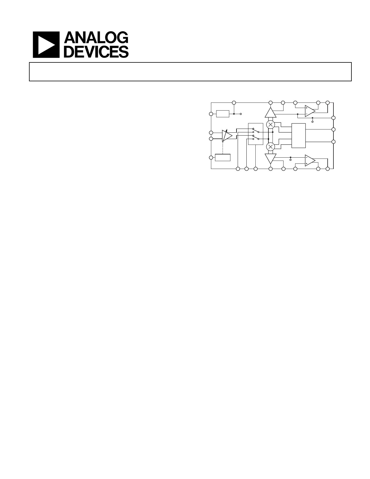
FUNCTIONAL BLOCK DIAGRAM
VREF
14
IMXO
8
IOFS
13
IAIN
6
IOPP IOPN
43
ENBL 15
BIAS
CELL
VREF
IFIP 11
IFIN 10
VGIN 17
GAIN
CONTROL
18 19
24
MXIP MXIN ENVG
DIVIDE
BY 2
PHASE
SPLITTER
VCMO
AD8348
5 VCMO
1 LOIP
28 LOIN
VCMO
21
QXMO
16
QOFS
Figure 1.
23
QAIN
25 26
QOPP QOPN
Separate I- and Q-channel baseband amplifiers follow the baseband
outputs of the mixers. The voltage applied to the VCMO pin sets
the dc common-mode voltage level at the baseband outputs.
Typically, VCMO is connected to the internal VREF voltage, but
it can also be connected to an external voltage. This flexibility
allows the user to maximize the input dynamic range to the ADC.
Connecting a bypass capacitor at each offset compensation input
(IOFS and QOFS) nulls dc offsets produced in the mixer. Offset
compensation can be overridden by applying an external voltage
at the offset compensation inputs.
The mixers’ outputs are brought off-chip for optional filtering
before final amplification. Inserting a channel selection filter
before each baseband amplifier increases the baseband amplifiers’
signal handling range by reducing the amplitude of high level,
out-of-channel interferers before the baseband signal is fed into
the I/Q baseband amplifiers. The single-ended mixer output is
amplified and converted to a differential signal for driving ADCs.
One Technology Way, P.O. Box 9106, Norwood, MA 02062-9106, U.S.A.
Tel: 781.329.4700
www.analog.com
Fax: 781.461.3113
©2006 Analog Devices, Inc. All rights reserved.
1 page 
AD8348
Parameter
IF FRONT END WITHOUT VGA
Input Impedance
Conversion voltage Gain
3 dB Output Bandwidth
IF Gain Flatness
Input 1 dB Compression Point (P1dB)
Third-Order Input Intercept (IIP3)
LO Leakage
Demodulation Bandwidth
Quadrature Phase Error
I/Q Amplitude Imbalance
Noise Figure (Double Sideband)
I/Q BASEBAND AMPLIFIER
Gain
Bandwidth
Output DC Offset (Differential)
Output Common-Mode Offset
Group Delay Flatness
Input-Referred Noise Voltage
Output Swing Limit (Upper)
Output Swing Limit (Lower)
Peak Output Current
Input Impedance
Input Bias Current
RESPONSE FROM IF AND MX INPUTS TO
BASEBAND AMPLIFIER OUTPUT
Gain
CONTROL INPUT/OUTPUTS
VCMO Input Range
VREF Output Voltage
Gain Control Voltage Range
Gain Slope
Gain Intercept
Gain Control Input Bias Current
LO INPUTS
LOIP Input Return Loss
Conditions
From MXIP, MXIN to IMXO (QMXO),
ENVG = 0 V, IMXO/QMXO load = 1.5 kΩ
Measured differentially across MXIP/MXIN
Min
FIF = 380 MHZ ± 5%
FIF = 900 MHZ ± 5%
IF1 = 381 MHz, IF2 = 381.02 MHz
Each tone 10 dB below P1dB from
200 Ω source
Measured at MXIP/MXIN
Measured at IMXO, QMXO
Small signal 3 dB bandwidth
LO = 380 MHz (LOIP/LOIN 760 MHz,
single-ended)
−2
From 200 Ω source, FIF = 380 MHz
From IAIN to IOPP/IOPN and QAIN to QOPP/
QOPN, RLOAD = 2 kΩ, single-ended to ground
10 pF differential load
LO leakage offset corrected using 500 pF
capacitor on IOFS, QOFS (VIOPP − VIOPN)
(VIOPP + VIOPN)/2 − VCMO
0 MHz to 50 MHz
Frequency = 1 MHz
−50
−75
VS −1
IMXO and QMXO connected directly to
IAIN and QAIN, respectively
From MXIP/MXIN
From IFIP/IFIN, VGIN = 0.2 V
From IFIP/IFIN, VGIN = 1.2 V
VS = 5 V
VS = 2.7 V
VGIN
Linear extrapolation back to theoretical
gain at VGIN = 0 V
0.5
0.5
0.95
0.2
−55
55
LOIN ac-coupled to ground
(760 MHz applied to LOIP)
Typ Max Unit
200||1.5
10.5
75
0.1
0.15
−4
14
Ω||pF
dB
MHz
dB p-p
dB p-p
dBm
dBm
−70 dBm
−60 dBm
75 MHz
±0.5 +2 Degrees
0.25 dB
21 dB
20
125
±12
±35
3
8
1
50||1
2
dB
MHz
+50 mV
+75 mV
ns p-p
nV/√Hz
V
0.5 V
mA
kΩ||pF
μA
30.5 dB
45.5 dB
1.5 dB
1 4V
1 1.7 V
1 1.05 V
1.2 V
−50 −45 dB/V
61 67 dB
1 μA
−6 dB
Rev. A | Page 4 of 28
5 Page 
AD8348
VPOS2
VREF
COM2
Figure 9. Circuit G
VPOS3
IMXO,
QMXO
COM3
Figure 10. Circuit H
VPOS3
MXIP
MXIN
COM3
Figure 11. Circuit I
Rev. A | Page 10 of 28
11 Page | ||
| Páginas | Total 29 Páginas | |
| PDF Descargar | [ Datasheet AD8348.PDF ] | |
Hoja de datos destacado
| Número de pieza | Descripción | Fabricantes |
| AD834 | 500 MHz Four-Quadrant Multiplier | Analog Devices |
| AD8340 | RF Vector Modulator | Analog Devices |
| AD8341 | 1.5GHz to 2.4GHz RF Vector Modulator | Analog Devices |
| AD8342 | Active Receive Mixer Low Frequency to 3.8 GHz | Analog Devices |
| Número de pieza | Descripción | Fabricantes |
| SLA6805M | High Voltage 3 phase Motor Driver IC. |
Sanken |
| SDC1742 | 12- and 14-Bit Hybrid Synchro / Resolver-to-Digital Converters. |
Analog Devices |
|
DataSheet.es es una pagina web que funciona como un repositorio de manuales o hoja de datos de muchos de los productos más populares, |
| DataSheet.es | 2020 | Privacy Policy | Contacto | Buscar |