|
|
|
PDF AD822 Data sheet ( Hoja de datos )
| Número de pieza | AD822 | |
| Descripción | Single Supply/ Rail-to-Rail Low Power FET-Input Op Amp | |
| Fabricantes | Analog Devices | |
| Logotipo | ||
Hay una vista previa y un enlace de descarga de AD822 (archivo pdf) en la parte inferior de esta página. Total 25 Páginas | ||
|
No Preview Available !
Data Sheet
FEATURES
True single-supply operation
Output swings rail-to-rail
Input voltage range extends below ground
Single-supply capability from 5 V to 30 V
Dual-supply capability from ±2.5 V to ±15 V
High load drive
Capacitive load drive of 350 pF, G = +1
Minimum output current of 15 mA
Excellent ac performance for low power
800 µA maximum quiescent current per amplifier
Unity-gain bandwidth: 1.8 MHz
Slew rate of 3 V/μs
Good dc performance
800 µV maximum input offset voltage
2 µV/°C typical offset voltage drift
25 pA maximum input bias current
Low noise
13 nV/√Hz at 10 kHz
No phase inversion
APPLICATIONS
Battery-powered precision instrumentation
Photodiode preamps
Active filters
12-bit to 14-bit data acquisition systems
Medical instrumentation
Low power references and regulators
GENERAL DESCRIPTION
The AD822 is a dual precision, low power FET input op amp
that can operate from a single supply of 5 V to 30 V or from
dual supplies of ±2.5 V to ±15 V. It has true single-supply capability
with an input voltage range extending below the negative rail,
allowing the AD822 to accommodate input signals below ground
while in the single-supply mode. Output voltage swing extends
to within 10 mV of each rail, providing the maximum output
dynamic range.
Offset voltage of 800 µV maximum, offset voltage drift of 2 µV/°C,
input bias currents below 25 pA, and low input voltage noise
provide dc precision with source impedances up to a gigaohm.
The 1.8 MHz unity-gain bandwidth, –93 dB total harmonic
distortion (THD) at 10 kHz, and 3 V/µs slew rate are provided
with a low supply current of 800 µA per amplifier.
Single-Supply, Rail-to-Rail
Low Power FET-Input Op Amp
AD822
CONNECTION DIAGRAM
OUT1 1
–IN1 2
+IN1 3
V– 4 AD822
8 V+
7 OUT2
6 –IN2
5 +IN2
Figure 1. 8-Lead PDIP (N Suffix);
8-Lead MSOP (RM Suffix);
and 8-Lead SOIC_N (R Suffix)
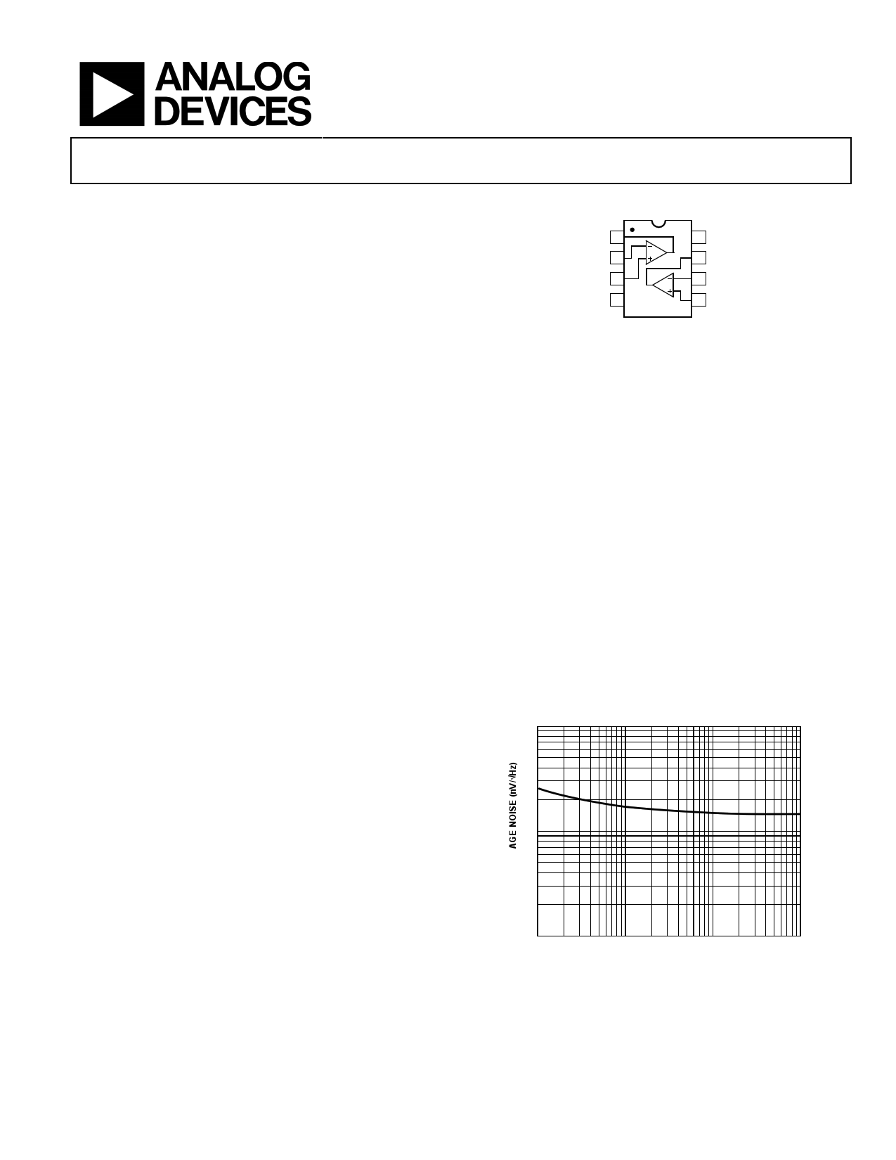
100
10
1
10 100 1k
FREQUENCY (Hz)
Figure 2. Input Voltage Noise vs. Frequency
10k
Rev. J
Document Feedback
Information furnished by Analog Devices is believed to be accurate and reliable. However, no
responsibilityisassumedbyAnalogDevices for itsuse,nor foranyinfringementsofpatentsor other
rights of third parties that may result from its use. Specifications subject to change without notice. No
license is granted by implication or otherwise under any patent or patent rights of Analog Devices.
Trademarksandregisteredtrademarksarethepropertyoftheirrespectiveowners.
One Technology Way, P.O. Box 9106, Norwood, MA 02062-9106, U.S.A.
Tel: 781.329.4700 ©1993–2015 Analog Devices, Inc. All rights reserved.
Technical Support
www.analog.com
1 page 
AD822
Data Sheet
SPECIFICATIONS
VS = 0 V, 5 V at TA = 25°C, VCM = 0 V, VOUT = 0.2 V, unless otherwise noted.
Table 1.
Parameter
DC PERFORMANCE
Initial Offset
Maximum Offset Over Temperature
Offset Drift
Input Bias Current
At TMAX
Input Offset Current
At TMAX
Open-Loop Gain
TMIN to TMAX
TMIN to TMAX
TMIN to TMAX
NOISE/HARMONIC PERFORMANCE
Input Voltage Noise
f = 0.1 Hz to 10 Hz
f = 10 Hz
f = 100 Hz
f = 1 kHz
f = 10 kHz
Input Current Noise
f = 0.1 Hz to 10 Hz
f = 1 kHz
Harmonic Distortion
f = 10 kHz
DYNAMIC PERFORMANCE
Unity-Gain Frequency
Full Power Response
Slew Rate
Settling Time
To 0.1%
To 0.01%
MATCHING CHARACTERISTICS
Initial Offset
Maximum Offset Over Temperature
Offset Drift
Input Bias Current
Crosstalk @ f = 1 kHz
Crosstalk @ f = 100 kHz
A Grade
B Grade
Test Conditions/Comments Min Typ
Max Min Typ
Max Unit
VCM = 0 V to 4 V
VOUT = 0.2 V to 4 V
RL = 100 kΩ
RL = 10 kΩ
RL = 1 kΩ
0.1
0.5
2
2
0.5
2
0.5
500 1000
400
80 150
80
15 30
10
0.8 0.1
1.2 0.5
2
25 2
5 0.5
20 2
0.5
500 1000
400
80 150
80
15 30
10
0.4 mV
0.9 mV
µV/°C
10 pA
2.5 nA
10 pA
nA
V/mV
V/mV
V/mV
V/mV
V/mV
V/mV
RL = 10 kΩ to 2.5 V
VOUT = 0.25 V to 4.75 V
VOUT p-p = 4.5 V
VOUT = 0.2 V to 4.5 V
VOUT = 0.2 V to 4.5 V
RL = 5 kΩ
RL = 5 kΩ
2
25
21
16
13
18
0.8
−93
1.8
210
3
1.4
1.8
3
−130
−93
1.0
1.6
20
2
25
21
16
13
18
0.8
−93
1.8
210
3
1.4
1.8
3
–130
–93
µV p-p
nV/√Hz
nV/√Hz
nV/√Hz
nV/√Hz
fA p-p
fA/√Hz
dB
MHz
kHz
V/µs
µs
µs
0.5 mV
1.3 mV
µV/°C
10 pA
dB
dB
Rev. J | Page 4 of 24
5 Page 
AD822
ABSOLUTE MAXIMUM RATINGS
Table 4.
Parameter
Supply Voltage
Internal Power Dissipation
8-Lead PDIP (N)
8-Lead SOIC_N (R)
8-Lead MSOP (RM)
Input Voltage1
Output Short-Circuit Duration
Differential Input Voltage
Storage Temperature Range (N)
Storage Temperature Range (R, RM)
Operating Temperature Range
A Grade and B Grade
Lead Temperature
(Soldering, 60 sec)
Rating
±18 V
Observe derating curves
Observe derating curves
Observe derating curves
((V+) + 0.2 V) to
((V−) − 20 V)
Indefinite
±30 V
–65°C to +125°C
–65°C to +150°C
–40°C to +85°C
260°C
1 See the Input Characteristics section.
Stresses at or above those listed under Absolute Maximum
Ratings may cause permanent damage to the product. This is a
stress rating only; functional operation of the product at these
or any other conditions above those indicated in the operational
section of this specification is not implied. Operation beyond
the maximum operating conditions for extended periods may
affect product reliability.
Data Sheet
THERMAL RESISTANCE
θJA is specified for the worst case conditions, that is, a device
soldered in a circuit board for surface-mount packages.
Table 5. Thermal Resistance
Package Type
8-lead PDIP (N)
8-lead SOIC_N (R)
8-lead MSOP (RM)
θJA Unit
90 °C/W
160 °C/W
190 °C/W
MAXIMUM POWER DISSIPATION
The maximum power that can be safely dissipated by the AD822 is
limited by the associated rise in junction temperature. For plastic
packages, the maximum safe junction temperature is 145°C. If
these maximums are exceeded momentarily, proper circuit
operation is restored as soon as the die temperature is reduced.
Leaving the device in the overheated condition for an extended
period can result in device burnout. To ensure proper operation, it
is important to observe the derating curves shown in Figure 27.
While the AD822 is internally short-circuit protected, this may not
be sufficient to guarantee that the maximum junction temperature
is not exceeded under all conditions. With power supplies ±12 V or
less at an ambient temperature of 25°C or less, if the output node is
shorted to a supply rail, then the amplifier is not destroyed, even if
this condition persists for an extended period.
ESD CAUTION
Rev. J | Page 10 of 24
11 Page | ||
| Páginas | Total 25 Páginas | |
| PDF Descargar | [ Datasheet AD822.PDF ] | |
Hoja de datos destacado
| Número de pieza | Descripción | Fabricantes |
| AD820 | FET Input Op Amp | Analog Devices |
| AD8200 | High Common-Mode Voltage/ Single Supply Difference Amplifier | Analog Devices |
| AD8202 | Single-Supply Difference Amplifier | Analog Devices |
| AD8203 | Single-Supply Difference Amplifier | Analog Devices |
| Número de pieza | Descripción | Fabricantes |
| SLA6805M | High Voltage 3 phase Motor Driver IC. |
Sanken |
| SDC1742 | 12- and 14-Bit Hybrid Synchro / Resolver-to-Digital Converters. |
Analog Devices |
|
DataSheet.es es una pagina web que funciona como un repositorio de manuales o hoja de datos de muchos de los productos más populares, |
| DataSheet.es | 2020 | Privacy Policy | Contacto | Buscar |