|
|
|
PDF ADV7150 Data sheet ( Hoja de datos )
| Número de pieza | ADV7150 | |
| Descripción | CMOS 220 MHz True-Color Graphics Triple 10-Bit Video RAM-DAC | |
| Fabricantes | Analog Devices | |
| Logotipo | ||
Hay una vista previa y un enlace de descarga de ADV7150 (archivo pdf) en la parte inferior de esta página. Total 30 Páginas | ||
|
No Preview Available !
a
CMOS 220 MHz True-Color Graphics
Triple 10-Bit Video RAM-DAC
ADV7150
FEATURES
220 MHz, 24-Bit (30-Bit Gamma Corrected) True Color
Triple 10-Bit “Gamma Correcting” D/A Converters
Triple 256 ؋ 10 (256 ؋ 30) Color Palette RAM
On-Chip Clock Control Circuit
Palette Priority Select Registers
RS-343A/RS-170 Compatible Analog Outputs
TTL Compatible Digital Inputs
Standard MPU l/O Interface
10-Bit Parallel Structure
8+2 Byte Structure
Programmable Pixel Port: 24-Bit, 15-Bit and
Programmable Pixel Port: 8-Bit (Pseudo)
Pixel Data Serializer
Multiplexed Pixel Input Ports; 1:1, 2:1, 4:1
+5 V CMOS Monolithic Construction
160-Lead Plastic Quad Flatpack (QFP)
Thermally Enhanced to Achieve JC < 1.0؇C/W
MODES OF OPERATION
24-Bit True Color (30-Bit Gamma Corrected)
@ 220 MHz
@ 170 MHz
@ 135 MHz
@ 110 MHz
@ 85 MHz
8-Bit Pseudo Color
15-Bit True Color
APPLICATIONS
High Resolution, True Color Graphics
Professional Color Prepress Imaging
GENERAL DESCRIPTION
The ADV7150 (ADV®) is a complete analog output, Video
RAM-DAC on a single CMOS monolithic chip. The part is spe-
cifically designed for use in high performance, color graphics
workstations. The ADV7150 integrates a number of graphic
functions onto one device allowing 24-bit direct True-Color op-
eration at the maximum screen update rate of 220 MHz. The
ADV7150 implements 30-bit True Color in 24-bit frame buffer
designs. The part also supports other modes, including 15-bit
True Color and 8-bit Pseudo or Indexed Color. Either the Red,
Green or Blue input pixel ports can be used for Pseudo Color.
(Continued on page 12)
ADV is a registered trademark of Analog Devices, Inc.
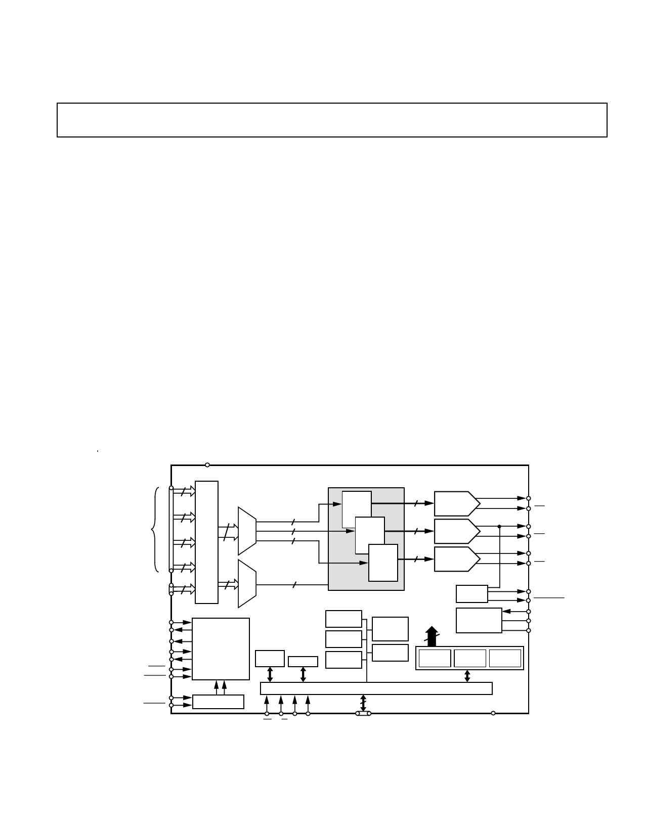
FUNCTIONAL BLOCK DIAGRAM
VAA
24
A
ADV7150
RED (R7–R0),
24
B
GREEN (G7–G0),
BLUE (B7–B0)
COLOR DATA
24
C
D
PALETTE
SELECTS
(PS0, PS1)
24
8
P
I
X
96
E MUX
L 4:1
P
O
R
T8
MUX
4:1
8
8
8
2
LOADIN
LOADOUT
PRGCKOUT
SCKIN
SCKOUT
SYNC
BLANK
CLOCK CONTROL
CLOCK DIVIDE
&
SYNCHRONIZATION
CIRCUIT
÷32 ÷16, ÷8, ÷4, ÷2
ADDRESS
REGISTER
ADDR
(A7–A0)
MODE
REGISTER
(MR1)
CLOCK
CLOCK
ECL TO CMOS
CE R/W C0 C1
256-COLOR/GAMMA
PALETTE RAM
RED
256 x 10
10
GREEN
256 x 10
10
BLUE
256 x 10
10
10-BIT
RED DAC
10-BIT
GREEN DAC
10-BIT
BLUE DAC
CONTROL REGISTERS
PIXEL MASK
REGISTER
TEST
REGISTERS
ID
REGISTER
COMMAND
REGISTERS
(CR1–CR3)
REVISION
REGISTER
SYNC
OUTPUT
DATA TO
PALETTES
30
VOLTAGE
REFERENCE
CIRCUIT
COLOR REGISTERS
RED
BLUE
GREEN
REGISTER REGISTER REGISTER
MPU PORT
10 (8+2)
D9 – D0
GND
IOR
IOR
IOG
IOG
IOB
IOB
IPLL
SYNCOUT
VREF
RSET
COMP
REV. A
Information furnished by Analog Devices is believed to be accurate and
reliable. However, no responsibility is assumed by Analog Devices for its
use, nor for any infringements of patents or other rights of third parties
which may result from its use. No license is granted by implication or
otherwise under any patent or patent rights of Analog Devices.
© Analog Devices, Inc., 1996
One Technology Way, P.O. Box 9106, Norwood, MA 02062-9106, U.S.A.
Tel: 617/329-4700
Fax: 617/326-8703
1 page 
CLOCK
LOADOUT
ADV7150
t10
LOADIN
PIXEL INPUT
DATA*
AN BN
CN DN
AN+1 BN+1
CN+1 DN+1
AN+2 BN+2
CN+2 DN+2
ODUIGTIPTUATLPINIPPEULTINTEO ANALOG
ANALOG
OUTPUT
DATA
IOR, IOR
IOG, IOG
IOB, IOB
IPLL, SYNCOUT
AN–1 BN–1 CN–1 DN–1 AN BN CN DN AN+1 BN+1 CN+1 DN+1 AN+2 BN+2 CN+2 DN+2
tPD
*INCLUDES PIXEL DATA (R0–R7, G0–G7, B0–B7); PALETTE SELECT INPUTS (PS0–PS1); BLANK; SYNC
Figure 4. Pixel Input to Analog Output Pipeline with Minimum LOADOUT to LOADIN Delay (4:1 Multiplex Mode)
CLOCK
LOADOUT
τ
τ– t11
LOADIN
PIXEL INPUT
DATA*
AN BN
CN DN
AN+1 BN+1
CN+1 DN+1
AN+2 BN+2
CN+2 DN+2
ANALOG
OUTPUT
DATA
POITPUDOETIGLAPIINUNTEATALLOINGPUT
IOR, IOR
IOG, IOG
IOB, IOB
AN–1 BN–1 CN–1 DN–1 AN BN CN DN AN+1 BN+1 CN+1 DN+1 AN+2 BN+2 CN+2 DN+2
IPLL, SYNCOUT
tPD
*INCLUDES PIXEL DATA (R0–R7, G0–G7, B0–B7); PALETTE SELECT INPUTS (PS0–PS1); BLANK; SYNC
Figure 5. Pixel Input to Analog Output Pipeline with Maximum LOADOUT to LOADIN Delay (4:1 Multiplex Mode)
REV. A
–5–
5 Page 
Mnemonic
R/W
C0, C1
IOR; IOR, IOG; IOG, IOB;
IOB
VREF
RSET
COMP
IPLL
VAA
GND
ADV7150
Function
Read/Write Control (TTL Compatible Input). This input determines whether data is
written to or read from the device’s registers and color palette RAM. R/W and CE must
be at Logic “0” to write data to the part. R/W must be at Logic “1” and CE at Logic
“0” to read from the device.
Command Controls (TTL Compatible Inputs). These inputs determine the type of read
or write operation being performed on the device over the databus (see Interface Truth
Table). Data on these inputs is latched on the falling edge of CE.
Red, Green and Blue Current Outputs (High Impedance Current Sources). These RGB
video outputs are specified to directly drive RS-343A and RS-170 video levels into dou-
bly terminated 75 Ω loads.
IOR, IOG and IOB are the complementary outputs of IOR, IOG and IOB. These out-
puts can be tied to GND if it is not required to use differential outputs.
Voltage Reference Input (Analog Input). An external 1.235 V voltage reference is re-
quired to drive this input. An AD589 (2-terminal voltage reference) or equivalent is rec-
ommended. (Note: It is not recommended to use a resistor network to generate the
voltage reference.)
Output Full-Scale Adjust Control (Analog Input). A resistor connected between this pin
and analog ground controls the absolute amplitude of the output video signal. The value
of RSET is derived from the full-scale output current on IOG according to the following
equations:
RSET (Ω) = C1 × VREF/IOG (mA); SYNC on GREEN
RSET (Ω) = C2 × VREF/IOG (mA); NO SYNC on GREEN.
Full-Scale output currents on IOR and IOB for a particular value of RSET are given by:
IOR (mA)= C2 × VREF(V)/RSET (Ω)
and
IOB (mA) = C2 × VREF (V)/RSET (Ω)
where C1 = 6,050; PEDESTAL = 7.5 IRE
where C1 = 5,723; PEDESTAL = 0 IRE
and
where C2 = 4,323; PEDESTAL = 7.5 IRE
where C1 = 3,996; PEDESTAL = 0 IRE.
Compensation Pin. A 0.1 µF capacitor should be connected between this pin and VAA.
Phase Lock Loop Output Current (High Impedance Current Source). This output is
used to enable multiple ADV7150s along with ADV7151s to be synchronized together
with pixel resolution when using an external PLL. This output is triggered either from
the falling edge of SYNC or BLANK as determined by bit CR21 of Command Register
2. When activated, it supplies a current corresponding to:
IPLL (mA) = 1,728 × VREF(V)/RSET (Ω)
When not using the IPLL function, this output pin should be tied to GND.
Power Supply (+5 V ± 5%). The part contains multiple power supply pins, all should be
connected together to one common +5 V filtered analog power supply.
Analog Ground. The part contains multiple ground pins, all should be connected
together to the system’s ground plane.
REV. A
–11–
11 Page | ||
| Páginas | Total 30 Páginas | |
| PDF Descargar | [ Datasheet ADV7150.PDF ] | |
Hoja de datos destacado
| Número de pieza | Descripción | Fabricantes |
| ADV7150 | CMOS 220 MHz True-Color Graphics Triple 10-Bit Video RAM-DAC | Analog Devices |
| ADV7151 | CMOS 220 MHz Pseudo-Color Graphics Triple 10-Bit Video RAM-DAC | Analog Devices |
| ADV7152 | CMOS 220 MHz True-Color Graphics Triple 10-Bit Video RAM-DAC | Analog Devices |
| Número de pieza | Descripción | Fabricantes |
| SLA6805M | High Voltage 3 phase Motor Driver IC. |
Sanken |
| SDC1742 | 12- and 14-Bit Hybrid Synchro / Resolver-to-Digital Converters. |
Analog Devices |
|
DataSheet.es es una pagina web que funciona como un repositorio de manuales o hoja de datos de muchos de los productos más populares, |
| DataSheet.es | 2020 | Privacy Policy | Contacto | Buscar |