|
|
|
PDF GA05JT03-46 Data sheet ( Hoja de datos )
| Número de pieza | GA05JT03-46 | |
| Descripción | Junction Transistor | |
| Fabricantes | GeneSiC | |
| Logotipo | ||
Hay una vista previa y un enlace de descarga de GA05JT03-46 (archivo pdf) en la parte inferior de esta página. Total 11 Páginas | ||
|
No Preview Available !
GA05JT03-46
Normally – OFF Silicon Carbide
Junction Transistor
Features
225°C maximum operating temperature
Gate Oxide Free SiC Switch
Exceptional Safe Operating Area
Excellent Gain Linearity
Temperature Independent Switching Performance
Low Output Capacitance
Positive Temperature Coefficient of RDS,ON
Suitable for Connecting an Anti-parallel Diode
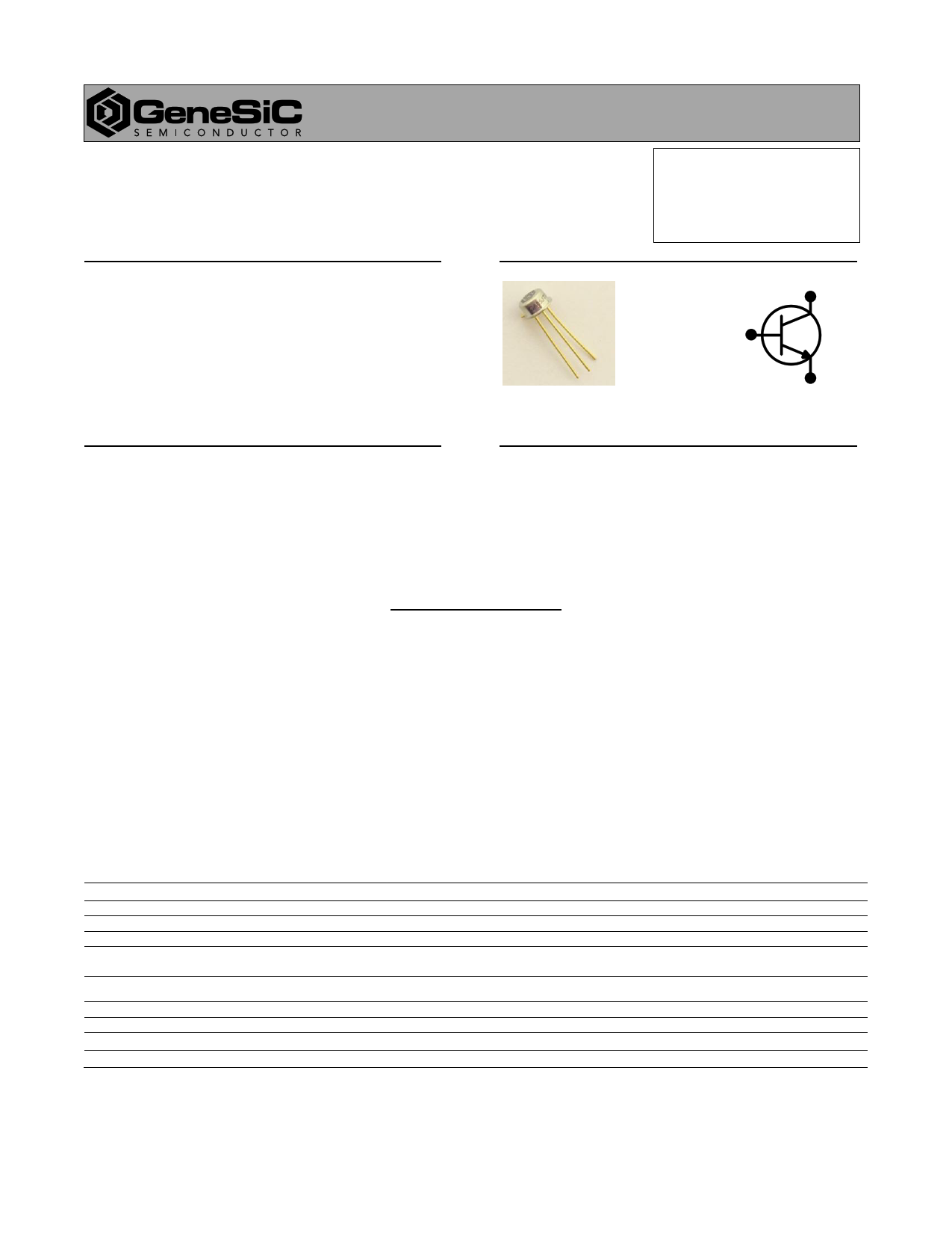
Package
RoHS Compliant
D
SG
TO-46
VDS =
RDS(ON)
=
ID (Tc = 25°C) =
hFE (Tc = 25°C) =
300 V
240 mΩ
9A
110
D
G
S
Advantages
Compatible with Si MOSFET/IGBT Gate Drive ICs
> 20 µs Short-Circuit Withstand Capability
Lowest-in-class Conduction Losses
High Circuit Efficiency
Minimal Input Signal Distortion
High Amplifier Bandwidth
Applications
Down Hole Oil Drilling
Geothermal Instrumentation
Solenoid Actuators
General Purpose High-Temperature Switching
Amplifiers
Solar Inverters
Switched-Mode Power Supply (SMPS)
Power Factor Correction (PFC)
Table of Contents
Section I: Absolute Maximum Ratings ...........................................................................................................1
Section II: Electrical Characteristics...............................................................................................................2
Section III: Dynamic Electrical Characteristics .............................................................................................2
Section IV: Figures ...........................................................................................................................................3
Section V: Driving the GA05JT03-46...............................................................................................................7
Section VI: Package Dimensions ................................................................................................................. 10
Section VII: SPICE Model Parameters ......................................................................................................... 11
Section I: Absolute Maximum Ratings
Parameter
Drain – Source Voltage
Continuous Drain Current
Continuous Gate Current
Turn-Off Safe Operating Area
Short Circuit Safe Operating Area
Reverse Gate – Source Voltage
Reverse Drain – Source Voltage
Power Dissipation
Storage Temperature
Symbol
VDS
ID
IGM
RBSOA
SCSOA
VSG
VSD
Ptot
Tstg
Conditions
VGS = 0 V
TJ = 225°C, TC = 25°C
TVJ = 225°C, IG = 0.5 A,
Clamped Inductive Load
TVJ = 225°C, IG = 0.5 A, VDS = 200 V,
Non Repetitive
TJ = 225°C, TC = 25°C
Value
300
5.8
0.5
ID,max = 9
@ VDS ≤ VDSmax
>20
30
25
20
-55 to 225
Unit
V
A
A
A
µs
V
V
W
°C
Notes
Fig. 21
Fig. 19
Fig. 16
Dec 2014
http://www.genesicsemi.com/high-temperature-sic/high-temperature-sic-junction-transistors/
Pg 1 of 10
1 page 
GA05JT03-46
Figure 13: Typical Turn On Energy Losses and Switching
Times vs. Drain Current
Figure 14: Typical Turn Off Energy Losses and Switching
Times vs. Drain Current
Figure 15: Typical Hard Switched Device Power Loss vs.
Switching Frequency 2
Figure 16: Power Derating Curve
Figure 17: Drain Current Derating vs. Temperature
Figure 18: Forward Bias Safe Operating Area at Tc= 25 oC
2 – Representative values based on device conduction and switching loss. Actual losses will depend on gate drive conditions, device load, and circuit topology.
Dec 2014
http://www.genesicsemi.com/high-temperature-sic/high-temperature-sic-junction-transistors/
Pg 5 of 10
5 Page 
Section VII: SPICE Model Parameters
GA05JT03-46
This is a secure document. Please copy this code from the SPICE model PDF file on our website
(http://www.genesicsemi.com/images/hit_sic/sjt/GA05JT03-46_SPICE.pdf) into LTSPICE (version 4) software for simulation of the GA05JT03-
46.
* MODEL OF GeneSiC Semiconductor Inc.
*
* $Revision: 1.0
$
* $Date: 12-DEC-2014
$
*
* GeneSiC Semiconductor Inc.
* 43670 Trade Center Place Ste. 155
* Dulles, VA 20166
*
* COPYRIGHT (C) 2014 GeneSiC Semiconductor Inc.
* ALL RIGHTS RESERVED
*
* These models are provided "AS IS, WHERE IS, AND WITH NO WARRANTY
* OF ANY KIND EITHER EXPRESSED OR IMPLIED, INCLUDING BUT NOT LIMITED
* TO ANY IMPLIED WARRANTIES OF MERCHANTABILITY AND FITNESS FOR A
* PARTICULAR PURPOSE."
* Models accurate up to 2 times rated drain current.
*
.model GA05JT03 NPN
+ IS
9.8338E-48
+ ISE
1.0733E-26
+ EG
3.23
+ BF
135
+ BR
0.55
+ IKF
200
+ NF
1
+ NE
2.
+ RB
14.5
+ IRB
0.002
+ RBM
0.37
+ RE
0.01
+ RC
0.23
+ CJC
2.16E-10
+ VJC
3.656
+ MJC
0.4717
+ CJE
5.021E-10
+ VJE
2.95
+ MJE
0.4867
+ XTI
3
+ XTB
-1.0
+ TRC1
1.050E-2
+ VCEO
300
+ ICRATING
9
+ MFG
GeneSiC_Semiconductor
*
* End of GA05JT03 SPICE Model
Dec 2014
http://www.genesicsemi.com/commercial-sic/sic-junction-transistors/
Pg1 of 1
11 Page | ||
| Páginas | Total 11 Páginas | |
| PDF Descargar | [ Datasheet GA05JT03-46.PDF ] | |
Hoja de datos destacado
| Número de pieza | Descripción | Fabricantes |
| GA05JT03-46 | Junction Transistor | GeneSiC |
| Número de pieza | Descripción | Fabricantes |
| SLA6805M | High Voltage 3 phase Motor Driver IC. |
Sanken |
| SDC1742 | 12- and 14-Bit Hybrid Synchro / Resolver-to-Digital Converters. |
Analog Devices |
|
DataSheet.es es una pagina web que funciona como un repositorio de manuales o hoja de datos de muchos de los productos más populares, |
| DataSheet.es | 2020 | Privacy Policy | Contacto | Buscar |