|
|
|
PDF MAP3205 Data sheet ( Hoja de datos )
| Número de pieza | MAP3205 | |
| Descripción | 4-channel LED Driver | |
| Fabricantes | MagnaChip | |
| Logotipo | ||
Hay una vista previa y un enlace de descarga de MAP3205 (archivo pdf) en la parte inferior de esta página. Total 13 Páginas | ||
|
No Preview Available !
Confidential
Final Datasheet Version 1.0
MAP3205
4-channel LED Driver for High Brightness LEDs
General Description
The MAP3205 is a 4-channel LED driver optimized
for LED backlight application targeting mid and large
size LCD module. It uses the boost MOSFET
externally and 4-channel current sources internally for
driving high brightness white LEDs.
Input voltage of the MAP3205 is ranged from 8V to
36V and max. LED current is 150mA per channel. It
can increase the output voltage depending on the
drain voltage rating of boost MOSFET.
It features PWM dimming control, internal soft-start
and has unique adaptive internal OVP, boost MOSFET
OCP, LED short/open protection, SBD open protection
and UVLO.
Features
8V to 36V Input Voltage Range
Drive up to 4 Channels
Max. 150mA Output Current per Channel
Programmable Boost Switching Frequency :
200kHz to 500kHz
PWM Dimming : Up to 22kHz,
Min on-time : 20us
Analog Dimming
SBD Open Protection
Boost Over-Current Protection
Internal Adaptive Over-Voltage Protection
LED Short/Open Protection
UVLO
20 leads E-TSSOP and 20 leads SOIC
The MAP3205 is available in 20 leads E-TSSOP and
20 leads SOIC package with Halogen-free (fully RoHS
compliant).
Applications
High Brightness white LED backlighting for mid
and large size LCD module
General LED lighting applications
Ordering Information
Part Number
MAP3205SIRH
MAP3205TERH
Top
Marking
MAP3205
MAP3205
Ambient
Temperature Range
-40℃ to +85℃
-40℃ to +85℃
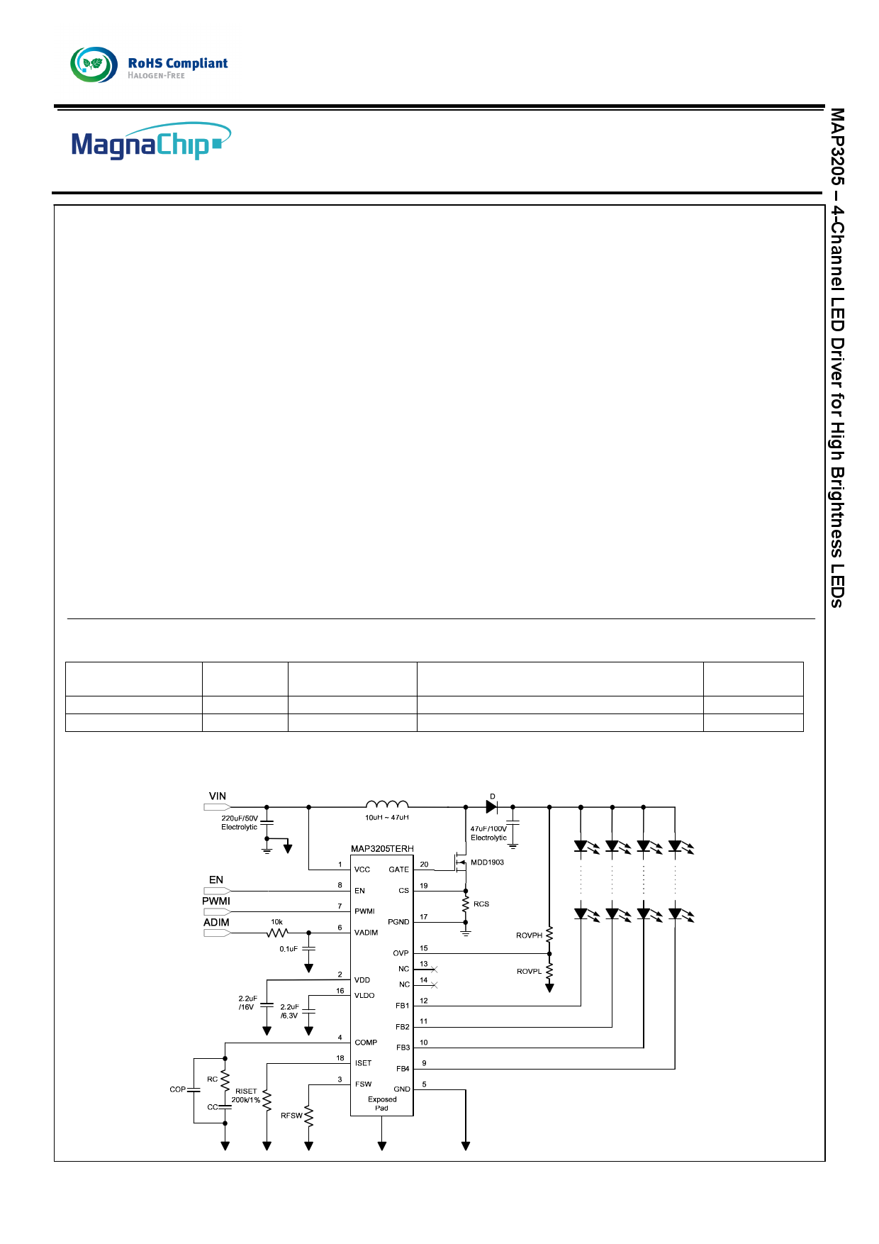
Typical Application
Package
20 leads SOIC
20 leads TSSOP with E-Pad
RoHS Status
Halogen Free
Halogen Free
Oct 21th 2011.
1 page 
Confidential
Final Datasheet Version 1.0
Electrical Characteristics
Unless noted, VIN = 12V, CIN = 1.0µF, and typical values are tested at TA = 25°C. Boldface values indicate -40°C to +85°C of TA.
3
Parameter
Test Condition
Min Typ Max
General Input Output
VCC Input Voltage Range
8.0 36
IQ Quiescent Current
IGND
Ground Pin Current in
Shutdown
VCC = 12V, VEN = 5V, VPWMI = 0V
VCC = 12V, VEN = 0V, VPWMI = 0V
3.5
100
VEN
Logic Input Level on
EN pin
VEN_L : Logic Low
VEN_H : Logic High
0.8
2.0
REN_PULLDOWN Pull-down resistor on EN pin
500
VUVLO
Under-Voltage Lock-Out
Threshold Voltage on VDD pin
Release UVLO
Lockout UVLO
6.0 7.5
4.0 5.5
Oscillator
fSW
Internal Oscillator
Frequency
RFSW=250kΩ
RFSW=100kΩ
180 200 220
425 500 575
Dmax
Maximum Duty Cycle
86 90
Reference
VVDD
10V LDO Voltage
VCC > 12V, No load current
9 10 11.5
VLDO
5V LDO Voltage
VCC > 8V, No load current
4.5 5 5.5
Boost MOSFET Driver
VGATE
Gate Drive Voltage
VCC > 12V
9 10 11.5
ISINK Gate Sink Current
VDD = 10V, VGATE = 4V
0.05 0.4
ISource
Gate Source Current
VDD = 10V, VGATE = 0V
0.05 0.4
tRISE Gate Output Rising Time
10nF load capacitance
500
tFALL Gate Output Falling Time
10nF load capacitance
500
Protection
TSD
VEXTOVP
VINTOVP
VLEDSHORT
VSBDOPEN
tSCP
VCS
Thermal Shutdown
Temperature
Over-Voltage Protection
Threshold Level on OVP pin
Internal Over-Voltage Protection
Threshold Level on FB pin
LED Short Protection
Threshold
SBD Open Protection
Threshold on OVP pin
LED Short Protection Time
Boost Over Current
Protection Threshold
Shutdown Temperature
Hysteresis, ΔTSD
Rising Over-Voltage Limit on OVP pin
Hysteresis, ΔVEXTOVP
Rising Over-Voltage Limit on FB pin (Note1)
Hysteresis, ΔVINTOVP (Note1)
FB1 ~ FB4
(Note1)
fSW=500kHz
Gate Duty-Cycle=90%
1.23
0.02
1.9
0.54
0.306
150
25
1.28
2.0
5.5
0.1
8.192
0.360
1.33
0.12
2.1
0.74
0.414
VLEDOPEN
LED Open Protection
Threshold
ILED=50mA
ILED=150mA
0.05
0.15
LED Current Sink Regulator
VFB1~4
IFB
Km
Minimum FB1~FB4 voltage for
the operation to sink 150mA
Current Accuracy
Current Matching(Note 2)
ILED=150mA
ILED=100mA
ILED=100mA
0.8
±3
±2.5
IFB_max
Current Sink max Current
VADIM=3V
150
VADIM
ADIM Input Voltage Range
13
PWM Interface
fPWM PWM dimming frequency
0.1 22
VPWMI
Logic Input Level on
PWMI pin
VPWMI_L : Logic Low
VPWMI_H : Logic High
0.8
2.3
IPWMI
Leakage Current on PWMI
pin
VPWMI=1V
4
tPWMON_MIN Minimum On-Duty
Note 1. No test on mass production
Note 2.
Km[%] = ± I max − I min ×100
I max + I min
fPWM=500Hz
20
Unit
V
mA
µA
V
kΩ
V
kHz
%
V
V
V
A
A
ns
ns
°C
V
V
V
V
ms
V
V
V
V
%
%
mA
V
kHz
V
µA
us
Oct 21th 2011.
5 Page 
Physical Dimensions
Confidential
Final Datasheet Version 1.0
Symbol
A
A1
A2
b
c
D
D1
E
E1
E2
e
L
L1
ө
20 Leads TSSOP
Dimension
Min Norm
0.00
0.80
0.19
0.09
6.40
2.20
6.40 BSC
4.30
1.50
0.65 BSC
0.45
1.00 REF
0°
Max
1.20
0.15
1.05
0.30
0.20
6.60
4.50
0.75
8°
Oct 21th 2011.
11 Page | ||
| Páginas | Total 13 Páginas | |
| PDF Descargar | [ Datasheet MAP3205.PDF ] | |
Hoja de datos destacado
| Número de pieza | Descripción | Fabricantes |
| MAP3201 | High current switch mode PWM LED Driver | MagnaChip |
| MAP3202 | High Efficiency Switch Mode LED Driver | MagnaChip |
| MAP3204 | 4-channel LED Driver | MagnaChip |
| MAP3204SIRH | 4-channel LED Driver | MagnaChip |
| Número de pieza | Descripción | Fabricantes |
| SLA6805M | High Voltage 3 phase Motor Driver IC. |
Sanken |
| SDC1742 | 12- and 14-Bit Hybrid Synchro / Resolver-to-Digital Converters. |
Analog Devices |
|
DataSheet.es es una pagina web que funciona como un repositorio de manuales o hoja de datos de muchos de los productos más populares, |
| DataSheet.es | 2020 | Privacy Policy | Contacto | Buscar |