|
|
|
PDF HS-26CLV32RH Data sheet ( Hoja de datos )
| Número de pieza | HS-26CLV32RH | |
| Descripción | Radiation Hardened 3.3V Quad Differential Line Receivers | |
| Fabricantes | Intersil | |
| Logotipo | ||
Hay una vista previa y un enlace de descarga de HS-26CLV32RH (archivo pdf) en la parte inferior de esta página. Total 6 Páginas | ||
|
No Preview Available !
DATASHEET
Radiation Hardened 3.3V Quad Differential Line
Receivers
HS-26CLV32RH, HS-26CLV32EH
The Intersil HS-26CLV32RH, HS-26CLV32EH are radiation
hardened 3.3V quad differential line receivers designed for
digital data transmission over balanced lines, in low voltage,
RS-422 protocol applications. Radiation hardened CMOS
processing assures low power consumption, high speed, and
reliable operation in the most severe radiation environments.
The HS-26CLV32RH, HS-26CLV32EH have an input sensitivity
of 200mV (typical) over a common-mode input voltage range
of -4V to +7V. The receivers are also equipped with input
fail-safe circuitry, which causes the outputs to go to a logic “1”
when the inputs are open. The device has unique inputs that
remain high impedance when the receiver is disabled or
powered-down, maintaining signal integrity in multi-receiver
applications.
Specifications for Rad Hard QML devices are controlled by the
Defense Logistics Agency Land and Maritime (DLA). The SMD
numbers listed must be used when ordering.
Related Literature
• For a full list of related documents, visit our website
- HS-26CLV32RH and HS-26CLV32EH product pages
Features
• Electrically screened to SMD # 5962-95689
• QML qualified per MIL-PRF-38535 requirements
• 1.2 micron radiation hardened CMOS
- Total dose . . . . . . . . . . . . . . . . . . . . . . . . . 300krad(Si) (max)
- Single event upset LET . . . . . . . . . . . . . 100MeV/mg/cm2)
- Single event latch-up immune
• Low stand-by current . . . . . . . . . . . . . . . . . . . . . . . 13mA (max)
• Operating supply range . . . . . . . . . . . . . . . . . . . . . 3.0V to 3.6V
• Enable input levels. . . . . . . . .VIH > 0.7 x VDD; VIL < 0.3 x VDD
• CMOS output levels . . . . . . . . . . . . . . VOH > 2.55V; VOL < 0.4V
• Input fail-safe circuitry
• High impedance inputs when disabled or powered-down
• Full -55°C to +125°C military temperature range
• Pb-free (RoHS compliant)
Applications
• Line receiver for MIL-STD-1553 serial data bus
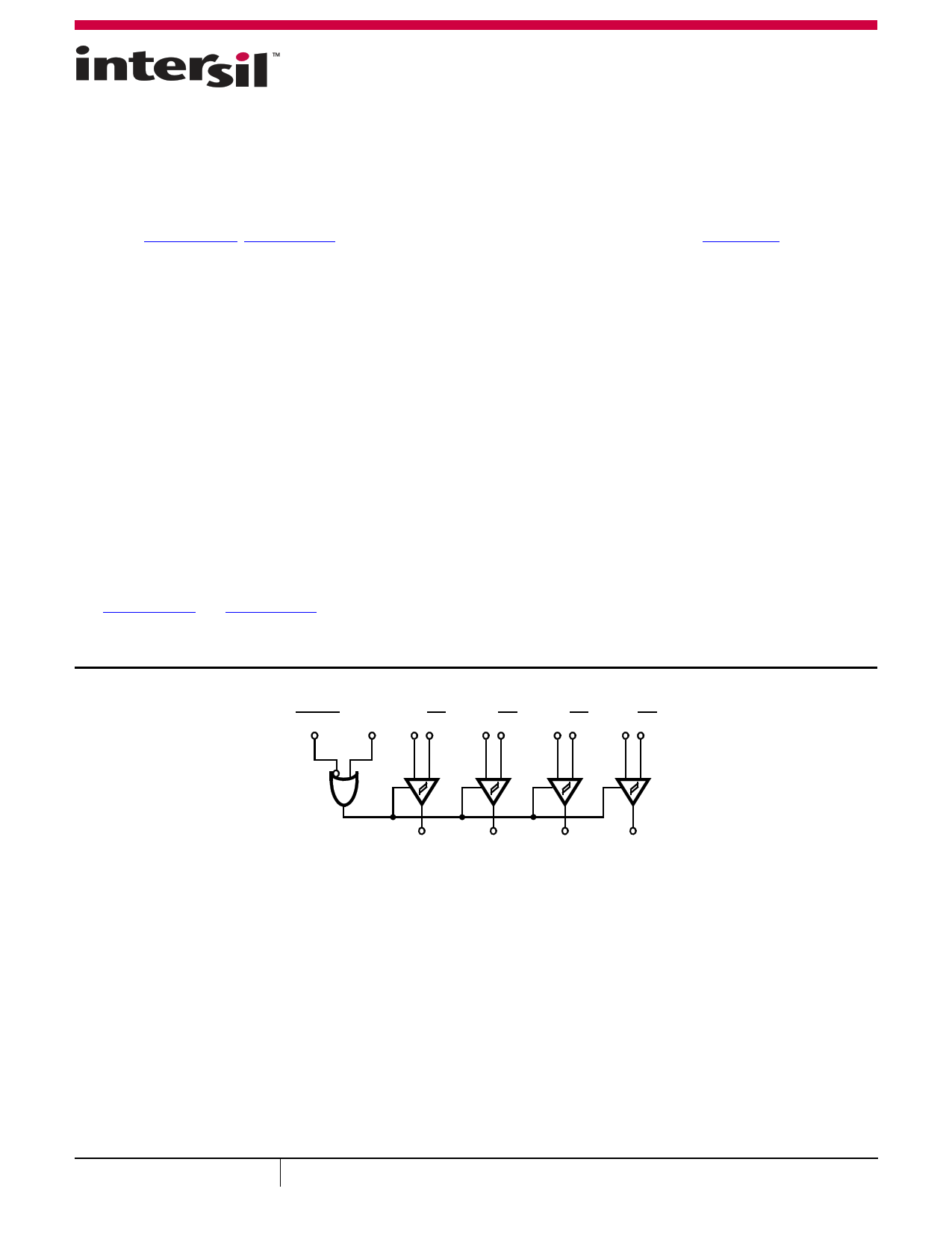
ENABLE ENABLE DIN DIN
CIN CIN
BIN BIN AIN AIN
+-
+-
+-
+-
DOUT
COUT
BOUT
AOUT
FIGURE 1. LOGIC DIAGRAM
February 6, 2017
FN4907.6
1 CAUTION: These devices are sensitive to electrostatic discharge; follow proper IC Handling Procedures.
1-888-INTERSIL or 1-888-468-3774 | Copyright Intersil Americas LLC 2000, 2008, 2009, 2012, 2013, 2017. All Rights Reserved
Intersil (and design) is a trademark owned by Intersil Corporation or one of its subsidiaries.
All other trademarks mentioned are the property of their respective owners.
1 page 
HS-26CLV32RH, HS-26CLV32EH
Package Outline Drawing
For the most recent package outline drawing, see K16.4.
K16.A
16 LEAD CERAMIC METAL SEAL FLATPACK PACKAGE
Rev 2, 1/10
0.015 (0.38) PIN NO. 1
0.008 (0.20) ID OPTIONAL 1
2
0.050 (1.27 BSC)
PIN NO. 1
ID AREA
0.440 (11.18)
MAX
0.005 (0.13)
MIN
4
0.022 (0.56)
0.015 (0.38)
TOP VIEW
0.115 (2.92)
0.045 (1.14)
0.045 (1.14)
0.026 (0.66) 6
-C-
SEATING AND
BASE PLANE
0.285 (7.24)
0.245 (6.22)
0.13 (3.30)
MIN
LEAD FINISH
SIDE VIEW
0.009 (0.23)
0.004 (0.10)
-D-
0.370 (9.40)
0.250 (6.35)
0.03 (0.76) MIN
-H-
0.006 (0.15) LEAD FINISH
0.004 (0.10)
BASE
METAL
0.009 (0.23)
0.004 (0.10)
0.019 (0.48)
0.015 (0.38)
0.0015 (0.04)
MAX
0.022 (0.56)
0.015 (0.38)
SECTION A-A
3
NOTES:
1. Index area: A notch or a pin one identification mark shall be located
adjacent to pin one and shall be located within the shaded area shown.
The manufacturer’s identification shall not be used as a pin one
identification mark. Alternately, a tab may be used to identify pin one.
2. If a pin one identification mark is used in addition to a tab, the limits
of the tab dimension do not apply.
3. The maximum limits of lead dimensions (section A-A) shall be
measured at the centroid of the finished lead surfaces, when solder
dip or tin plate lead finish is applied.
4. Measure dimension at all four corners.
5. For bottom-brazed lead packages, no organic or polymeric materials
shall be molded to the bottom of the package to cover the leads.
6. Dimension shall be measured at the point of exit (beyond the
meniscus) of the lead from the body. Dimension minimum shall
be reduced by 0.0015 inch (0.038mm) maximum when solder dip
lead finish is applied.
7. Dimensioning and tolerancing per ANSI Y14.5M - 1982.
8. Controlling dimension: INCH.
Submit Document Feedback
5
FN4907.6
February 6, 2017
5 Page | ||
| Páginas | Total 6 Páginas | |
| PDF Descargar | [ Datasheet HS-26CLV32RH.PDF ] | |
Hoja de datos destacado
| Número de pieza | Descripción | Fabricantes |
| HS-26CLV32RH | Radiation Hardened 3.3V Quad Differential Line Receivers | Intersil |
| Número de pieza | Descripción | Fabricantes |
| SLA6805M | High Voltage 3 phase Motor Driver IC. |
Sanken |
| SDC1742 | 12- and 14-Bit Hybrid Synchro / Resolver-to-Digital Converters. |
Analog Devices |
|
DataSheet.es es una pagina web que funciona como un repositorio de manuales o hoja de datos de muchos de los productos más populares, |
| DataSheet.es | 2020 | Privacy Policy | Contacto | Buscar |