|
|
|
PDF TW6872 Data sheet ( Hoja de datos )
| Número de pieza | TW6872 | |
| Descripción | Triple-Rate (SD/HD/3G) SDI Transmitter | |
| Fabricantes | Intersil | |
| Logotipo | ||
Hay una vista previa y un enlace de descarga de TW6872 (archivo pdf) en la parte inferior de esta página. Total 30 Páginas | ||
|
No Preview Available !
Triple-Rate (SD/HD/3G) SDI Transmitter with VC-2
Encoder and Audio Decoder
TW6872
The TW6872 is a triple-rate (SD/HD/3G) SDI transmitter. It
receives parallel BT.656/BT.1120/ASI video data from a
CMOS sensor/ISP chip. It also receives analog audio, or serial
digital audio. The TW6872 serializes the video and audio into
an SDI stream and transmits it to an SDI receiver via its
integrated cable driver.
In addition to the standard SDI format with uncompressed raw
video data, TW6872 can optionally compress video with a
visually lossless VC-2 compression algorithm to send the video
formats normally running at HD rate (1.5Gbps) on the cable at
SD rate (270Mbps), and therefore achieve longer cable reach.
Together, the TW6872 and Intersil’s TW6874 SDI receiver
provide a complete end-to-end SDI link solution and can
operate with or without VC-2 compression. Integrated
audio/video test patterns and PRBS checker ease system
design and implementation.
The TW6872 is available in a 76 Ld QFN. It is specified for
operation over the -40°C to +85°C ambient temperature
range and operates on two power supplies: 1V and 3.3V. A
single 27MHz crystal is used for all supported audio/video
operating modes.
Applications
• SD/HD/3G-SDI Camera
Features
• Triple-rate (SD/HD/3G) SDI transmitter for Standard
Definition (SD) and High Definition (HD), and 3G 10-bit
component video
• Encoding SDI standard of ITU-R BT.656/SMPTE 259M
Level C, ITU-R BT.1120/SMPTE ST 292, SMPTE 424M 10-bit
parallel component video inputs into 10-bit serial video
output
• BT.656/BT.1120 interface for CMOS sensor/ISP chip
• Asynchronous Serial Interface (ASI) for IEC 13818-1
compliant transport streams
• Integrated 75Ω cable driver with pre/de-emphasis
• Integrated VC-2 encoder allows transmission of HD video
over SD transmission lengths
• Analog audio and I2S serial audio input interfaces over
ancillary field
• Digital audio with PCM encoding for embedding audio
samples into the audio ancillary field of SDI stream
• Single 27MHz clock/crystal input
• Optional clock output for use as the ISP chip’s clock input to
enhance overall jitter
• PRBS7/23 and video/audio pattern generator
• I2C for external micro-controller interface
• Low power consumption
• Small footprint LTZ-QFN76L (9mm x9mm) package
• Pb-free (RoHS compliant)
d
u
m
m
y
May 23, 2014
FN8616.0
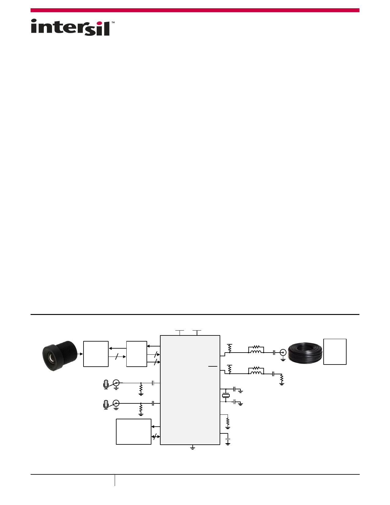
1.0V 3.3V
CMOS
SENSOR
CLK
DATA
CLKO
ISP
21
VD
3 I2S
4.7k
4.7k
2.2µF
AIN0
2.2µF
AIN1
TW6872
HOST
PROCESSOR
IRQ
I2C
SDO
SDO
XTI
XTO
RSET
3.3V
75
3.3V
75
22pF
0
open*
0
open*
1µF
1µF
75
75
COAX
TW6874S
DI RX
d
u
m
m
y
27MHz
22pF
1.6k
*Final RLN values pending optimization.
Place holder for inductor recommended.
AINN
2.2µF
FIGURE 1. TW6872 TYPICAL APPLICATION
1 CAUTION: These devices are sensitive to electrostatic discharge; follow proper IC Handling Procedures.
1-888-INTERSIL or 1-888-468-3774 | Copyright Intersil Americas LLC 2014. All Rights Reserved
Intersil (and design) is a trademark owned by Intersil Corporation or one of its subsidiaries.
I2C Bus™ is a trademark owned by NXP Semiconductors Netherlands, B.V. All other trademarks mentioned are the property of their respective owners.
1 page 
Pin Descriptions
PIN NUMBER
PIN NAME
PARALLEL DIGITAL VIDEO
22 VD19
21 VD18
19 VD17
18 VD16
17 VD15
16 VD14
15 VD13
14 VD12
12 VD11
11 VD10
9 VD9
8 VD8
6 VD7
5 VD6
4 VD5
3 VD4
1 VD3
75 VD2
73 VD1
72 VD0
7 VD_CLK
26
36
I2S AUDIO
62
63
65
CLKO
CLK108
ADAT
WCLK
ACLK
TW6872
TYPE
DESCRIPTION
Digital Input
Digital Input
Digital Input
Digital Input
Digital Input
Digital Input
Digital Input
Digital Input
Digital Input
Digital Input
Digital Input
Digital Input
Digital Input
Digital Input
Digital Input
Digital Input
Digital Input
Digital Input
Digital Input
Digital Input
Digital Input
Digital Output
Digital I/O
Parallel video data input.
HD/3G mode: Chroma (C) data
SD mode: not used
ASI mode: not used
Parallel video data input.
HD/3G mode: Luma (Y) data
SD mode: multiplexed BT.656 chroma/luma data
ASI mode: transport stream data input
Parallel video clock input.
3G mode: 148.5MHz
HD mode: 74.25MHz
SD mode: 27MHz
ASI mode: 27MHz
Clock source for the ISP in master mode.
Generated frequencies are:
27MHz
3G mode: 148.5MHz
HD mode: 74.25MHz or 148.5MHz
SD mode: 13.5MHz or 27MHz
Alternate 108MHz clock source for the ISP in master mode
Digital Input
Digital Input
Digital Input
Audio serial data input.
Audio word clock input.
Audio serial bit clock.
Submit Document Feedback
5
FN8616.0
May 23, 2014
5 Page 
TW6872
Video Input Modes
The TW6872 has a 20-bit wide parallel video input interface.
Through this interface, the input can be configured in one of two
modes by registers: either the BT.656/BT.1120 mode, or the
Asynchronous Serial Interface (ASI) mode. In the
BT.656/BT.1120 mode, the video data can be either YC
multiplexed (10-bit mode) or YC separated (20-bit mode). In the
ASI input mode, the ASI stream data comes in through the 10-bit
data bus running at 27MHz.
Video Bit Mapping
The ISP to TW6872 port mapping depends on the mode used as
described in the following. Figure 2 shows the timing relationship
for the input clock and data.
tSU tHD
FIGURE 2. VD_CLK TO VD[19:0] TIMING
BT.656 MODE
In BT.656 mode, only 10-bit data is used by the SD video
(NTSC/PAL). For either ASI or BT.656 formats, the 10-bit BT.656
video data use the lower word (bits 9:0) of the TW6872’s 20-bit
port and the upper word is not used per Figure 3.
The timing reference signals (TRS, consisting of SAV and EAV
codes) are inserted in the data stream to indicate the active
video time, as shown in Figure 4. The input timing is also
illustrated in Figure 4. The SAV and EAV sequences are shown in
Table 1.
TW6872
ISP
YC9
YC8
YC7
YC6
YC5
YC4
YC3
YC2
YC1
YC0
NOT
USED
VD19
VD18
VD17
VD16
VD15
VD14
VD13
VD12
VD11
VD10
VD9
VD8
VD7
VD6
VD5
VD4
VD3
VD2
VD1
VD0
FIGURE 3. BT.656 MAPPING
VD_CLK
VD[9:0] 3FFh 000h 000h XYZ 200h 040h
200h 040h 3FFh 000h 000h XYZ Cb0 Y0 Cr0 Y1 Cb2 Y2 Cr2 Y3
EAV CODE
SAV CODE
HACTIVE
.
FIELD
EVEN
EVEN
EVEN
EVEN
ODD
ODD
ODD
ODD
CONDITION
VTIME
Blank
Blank
Active
Active
Blank
Blank
Active
Active
HTIME
EAV
SAV
EAV
SAV
EAV
SAV
EAV
SAV
FIGURE 4. BT.656 FORMAT
TABLE 1. SAV/EAV CODE SEQUENCE FOR BT.656 AND BT.1120 DATA
FVH VALUE
SAV/EAV CODE SEQUENCE
F V H FIRST BYTE SECOND BYTE THIRD BYTE
1
1
1
0x3FF
0x000
0x000
1
1
0
0x3FF
0x000
0x000
1
0
1
0x3FF
0x000
0x000
1
0
0
0x3FF
0x000
0x000
0
1
1
0x3FF
0x000
0x000
0
1
0
0x3FF
0x000
0x000
0
0
1
0x3FF
0x000
0x000
0
0
0
0x3FF
0x000
0x000
FOURTH BYTE
0x3C4
0x3B0
0x368
0x31C
0x2D8
0x2AC
0x274
0x200
Submit Document Feedback 11
FN8616.0
May 23, 2014
11 Page | ||
| Páginas | Total 30 Páginas | |
| PDF Descargar | [ Datasheet TW6872.PDF ] | |
Hoja de datos destacado
| Número de pieza | Descripción | Fabricantes |
| TW6872 | Triple-Rate (SD/HD/3G) SDI Transmitter | Intersil |
| TW6874 | Quad (SD/HD) SDI Receiver | Intersil |
| Número de pieza | Descripción | Fabricantes |
| SLA6805M | High Voltage 3 phase Motor Driver IC. |
Sanken |
| SDC1742 | 12- and 14-Bit Hybrid Synchro / Resolver-to-Digital Converters. |
Analog Devices |
|
DataSheet.es es una pagina web que funciona como un repositorio de manuales o hoja de datos de muchos de los productos más populares, |
| DataSheet.es | 2020 | Privacy Policy | Contacto | Buscar |