|
|
PDF BU7150NUV Data sheet ( Hoja de datos )
| Número de pieza | BU7150NUV | |
| Descripción | Headphone Amplifier | |
| Fabricantes | ROHM Semiconductor | |
| Logotipo | ||
Hay una vista previa y un enlace de descarga de BU7150NUV (archivo pdf) en la parte inferior de esta página. Total 22 Páginas | ||
|
No Preview Available !
Compact Headphone Amplifiers
Headphone Amplifier
Designed for 0.93V Low Voltage Operation
BU7150NUV
No.15102EET01
●Description
BU7150NUV is Audio Amplifier designed for Single-cell battery operated audio products (VDD = 0.93 ~ 3.5V, at Ta=0~85°C).
BU7150NUV can be selected in single-ended mode for stereo headphone and BTL mode for mono speaker operations. For
BU7150NUV at VDD = 1.5V, THD+N = 1%, the output power is 14mW at RL = 16Ω in single-ended mode and the output
power is 85mW at RL = 8Ω in BTL mode.
●Features
1) Wide battery operation Voltage (0.93V~3.5V, Ta=0~85°C) (1.03V~3.5V, Ta= -40~85°C)
2) BU7150NUV can be selected in single-ended mode for stereo headphone and BTL mode for mono speaker operation
3) Unity-gain stability
4) Click and pop-noise reduction circuit built-in
5) Shutdown mode(Low power mode)
6) High speed turn-on mute mode
7) Thermal shutdown protection circuit
8) Power-on reset circuit not sensed during start-up slew rate of supply voltage
9) Small package (VSON010V3030)
●Applications
Noise-canceling headphone, IC recorder, Mobile phone, PDA, Electronic toys etc..
●Absolute Maximum Ratings (Ta=25℃)
Parameter
Symbol
Ratings
Unit
Supply Voltage
VDD
4.5
V
Input Voltage
VIN VSS-0.3~VDD+0.3
V
Input Current
IIN -10~10 mA
Power Dissipation
PD 560 * mW
Storage Temperature Range
TSTG
-55~+150
°C
*For operating over 25°C, de-rate the value at 5.6mW/°C.
This value is for IC mounted on 74.2 mm x 74.2mm x 1.6mm glass-epoxy PCB of single-layer.
●Operating conditions
Parameter
Ratings
Symbol
Min. Typ. Max.
Unit
Operation Temperature Range
TOPR -40
-
85 °C
Supply Voltage (Note 1,2)
VDD 0.93
-
3.5 V
Note 1: If the supply voltage is 0.93V, BU7150NUV does not operate at less than 0°C.
If the supply voltage is more than 1.03V, BU7150NUV operates until -40°C.
(But, it is not the one which guarantees the standard value for electric characteristics.)
Note 2: Ripple in power supply line should not exceed 400mVP-P.(VDD=1.5 V, Ta=25°C )
www.rohm.com
© 2015 ROHM Co., Ltd. All rights reserved.
1/18
2015.1 - Rev.E
1 page 
BU7150NUV
Technical Note
140 SE mode
120
100
80
60 THD+N = 10%
40
THD+N = 1%
20
0
0 12 34
Supply Voltage [V]
Fig. 18 Maxim um output Power vs . Supply Voltage
40
SE mode
35 Zoom up
30
25
20
15
THD+N = 10%
10
THD+N = 1%
5
0
0.0 0.5 1.0 1.5 2.0
Supply Voltage [V]
Fig. 20 Maxim um output Power vs . Supply Voltage
0
-10 VDD=1.5V, Input=200m VP-P,
SE m ode, Input Term inated into 10Ω
-20
-30
-40
-50
-60
-70
-80
-90
10
100 1k 10k
Frequency [Hz]
Fig. 22 PSRR vs . Frequency
100k
0
-10 VDD=1.2V, Input=200m VP-P,
SE m ode, Input Term inated into 10Ω
-20
-30
-40
-50
-60
-70
-80
-90
10
100 Freque1nkcy [Hz] 10k
Fig. 24 PSRR vs . Frequency
100k
1000
900 BTL m ode
800
700
600
500
400
THD+N = 10%
300
200 THD+N = 1%
100
0
0 1 23 4
Supply Voltage [V]
Fig. 19 Maxim um output Power vs . Supply Voltage
200
180 BTL m ode
Zoom up
160
140
120
100
80
60 THD+N = 10% × :WC(PO=70m W
TH D +N =1 % )
40
THD+N = 1%
20
0
0.0 0.5 1.0 1.5 2.0
Supply Voltage [V]
Fig. 21 Maxim um output Power vs . Supply Voltage
0
-10 VDD=1.5V, Input=200m VP-P,
BTL m ode, Input Term inated into 10Ω
-20
-30
-40
-50
-60
-70
-80
-90
10
100 1k 10k
Frequency [Hz]
Fig. 23 PSRR vs . Frequency
100k
0
-10 VDD=1.2V, Input=200m VP-P,
BTL m ode, Input Term inated into 10Ω
-20
-30
-40
-50
-60
-70
-80
-90
10
100 Freque1nkcy [Hz] 10k
Fig. 25 PSRR vs . Frequency
100k
www.rohm.com
© 2015 ROHM Co., Ltd. All rights reserved.
5/18
2015.1 - Rev.E
5 Page 
BU7150NUV
Technical Note
[About Time until Signal Output]
BU7150NUV need wait-time for BIAS charge sweep time and pop-noise reduction.
In the Fig. 37, Ts1 is BIAS charge sweep time from power on or SDB=H. Ts2 is time until signal output from power on or
SDB=H. Also, in the Fig. 38, Tb1 is BIAS charge sweep time from power on. Tb2 is time until signal output from power on.
Tb3 is BIAS charge sweep time from SDB=H. Tb4 is time until signal output from SDB=H.
These values are decided equation (1) ~ (6). However, BIAS charge sweep time (Ts1, Tb1, Tb3) have uneven ±50%, and
wait-time (70msec) is 40msec ~ 126msec for process parameter distribution. (Ta=25°C)
Ts1 =
VDD× CBYPASS
2.5 ×10 -6
[sec] ・・・
(1)
Ts2 = Ts1+ 0.07[sec] ・・・( 2)
Tb1 =
( )VDD + 2 × CBYPASS
27.5×10 -6
[sec] ・・・
(3)
Tb2 = Tb1+ 0.07[sec] ・・・( 4)
Tb3
=
VDD× CBYPASS
27.5×10 -6
[sec] ・・・
(5)
Tb4 = Tb3 + 0.07[sec] ・・・( 6)
In the Fig. 38, Tb1 and Tb3 is differ value, because BU7150NUV’s default is single-ended mode. BU7150NUV need
BYPASS>100mV to recognize for BTL mode.
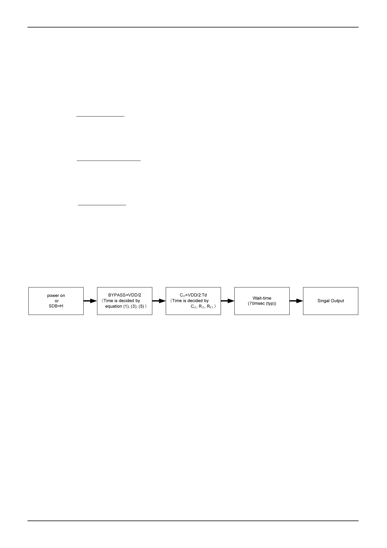
Also, Td is delay time to CI1=VDD/2 from BYPASS=VDD/2. Td is decided by CI1, RI1, and RF1.
Fig. 39 Flow of Time until Signal Output
www.rohm.com
© 2015 ROHM Co., Ltd. All rights reserved.
11/18
2015.1 - Rev.E
11 Page | ||
| Páginas | Total 22 Páginas | |
| PDF Descargar | [ Datasheet BU7150NUV.PDF ] | |
Hoja de datos destacado
| Número de pieza | Descripción | Fabricantes |
| BU7150NUV | Headphone Amplifier | ROHM Semiconductor |
| Número de pieza | Descripción | Fabricantes |
| SLA6805M | High Voltage 3 phase Motor Driver IC. |
Sanken |
| SDC1742 | 12- and 14-Bit Hybrid Synchro / Resolver-to-Digital Converters. |
Analog Devices |
|
DataSheet.es es una pagina web que funciona como un repositorio de manuales o hoja de datos de muchos de los productos más populares, |
| DataSheet.es | 2020 | Privacy Policy | Contacto | Buscar |
