|
|
PDF IR35203 Data sheet ( Hoja de datos )
| Número de pieza | IR35203 | |
| Descripción | 6+1 Dual Output Digital Multi-Phase Controller | |
| Fabricantes | International Rectifier | |
| Logotipo |  |
|
Hay una vista previa y un enlace de descarga de IR35203 (archivo pdf) en la parte inferior de esta página. Total 30 Páginas | ||
|
No Preview Available !
6+1 Dual Output Digital Multi-Phase Controller
IR35203
FEATURES
Ultra Low Quiescent Power Dual output 6+1 phase
PWM Controller
Intel® VR12 Rev 1.7, VR12.5 Rev 1.5, IMVP8 Rev
1.2, and Memory VR modes
Switching frequency from 194KHz to 2MHz per
phase in 56 steps
IR Efficiency Shaping Features including Dynamic
Phase Control and Automatic Power State Switching
Programmable 1-phase or 2-phase operation for
Light Loads and Active Diode Emulation for very
Light Loads
IR Adaptive Transient Algorithm (ATA) on both loops
minimizes output bulk capacitors and system cost
Auto-Phase Detection with PID Coefficient auto-
scaling
Fault Protection: OVP, UVP, OCP, OTP, CAT_FLT
I2C/SMBus/PMBus system interface for reporting of
Temperature, Voltage, Current & Power telemetry for
both loops
Multiple Time Programming (MTP) with integrated
charge pump for easy non-volatile programming
Compatible with 3.3V tri-state drivers
+3.3V supply voltage; -40oC to 85oC ambient
operation; -40oC to 125oC junction
Pb-Free, RoHS, 6x6mm 48-pin, 0.4mm pitch QFN
APPLICATIONS
Intel® VR12, VR12.5 and IMVP8 (overclocking only)
based systems
Servers and High End Desktop CPU VRs
High Performance Graphics Processors, Memory VR
DESCRIPTION
The IR35203 is a dual-loop digital multi-phase
buck controller designed for CPU voltage
regulation, and is fully compliant with Intel® VR12
Rev 1.7, VR12.5 Rev 1.5, IMVP82 Rev 1.2
specifications.
The IR35203 includes IR’s Efficiency Shaping
Technology to deliver exceptional efficiency at
minimum cost across the entire load range. IR’s
Dynamic Phase Control adds/drops phases based
upon load current. The IR35203 can be configured
to enter 1 or 2-phase PS1 operation and active
diode emulation mode automatically or by
command.
IR’s unique Adaptive Transient Algorithm (ATA),
based on proprietary non-linear digital PWM
algorithms, minimizes output bulk capacitors.
IR35203 has 127 possible address values for both
the PMBus and I2C bus interfaces. The device
configuration can be easily defined using the IR
PowIRCenter GUI, and is stored in the on-chip
Non-Volatile Memory (NVM). This reduces external
components and minimizes the package size.
The IR35203 provides extensive OVP, UVP, OCP,
OTP & CAT_FLT fault protection, and includes
thermistor based temperature sensing or per
phase temperature reporting when using the IR
powIRstage. The controller is designed to work
with either Rdson current sense PowIRstages or
with DCR current sense.
The IR35203 also includes numerous VR design
simplifying and differentiating features, like register
diagnostics, which enable fast time-to-market.
ORDERING INFORMATION
Base Part
Number
IR35203
Package Type
48-pin, QFN 6 mm x 6 mm
Standard Pack
Form
Quantity
Tape and Reel
3000
Orderable
Part Number
IR35203MxxyyTRP1
IR35203
48-pin, QFN 6 mm x 6 mm
Tape and Reel
3000
IR35203MTRPBF
IR35203
48-pin, QFN 6 mm x 6 mm
Tray
4900
IR35203MTYPBF
Notes:
1.
2.
Customer Specific Configuration File, where xx = Customer ID and yy = Configuration File (Codes assigned by IR Marketing).
IR35203 is not intended for application where ultra low power PS4 shutdown functionality is required.
1 www.irf.com | © 2016 International Rectifier
February 8, 2016 | V1.5
1 page 
6+1 Dual Output Digital Multi-Phase Controller
IR35203
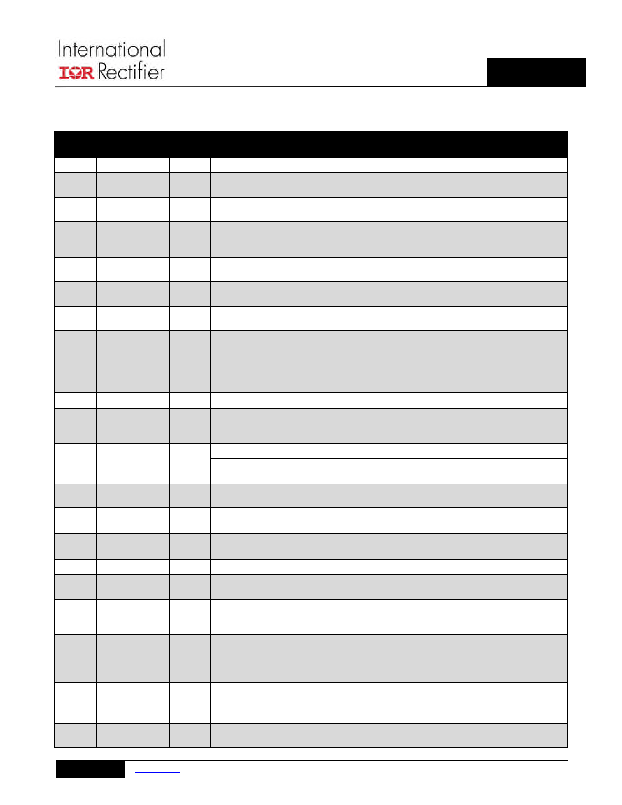
PIN DESCRIPTIONS
PIN#
1
2
3
4
5
6
7
8
9
10
11
12
13
14
15
16
17
18
19
20
PIN NAME TYPE
PIN DESCRIPTION
ISEN6
RCSP
RCSM
VRDY2
VSEN
VRTN
I_IN
TSEN1
CFILT
VRDY1
EN_L2
CAT_FLT
VINSEN
PIN_ALERT#
SV_ALERT#
SV_CLK
SV_DIO
VRHOT_ICRIT#
EN
ADDR_PROT
SM_ALERT#
A [I]
A [O]
A [O]
D [O]
A [I]
A [I]
A [I]
A [I]
A [O]
D [O]
D[I]
D[O]
A [I]
D [O]
D [O]
D [I]
D [B]
D [O]
D [I]
D [B]/
D [O]
Phase 6 Current Sense Input. Phase 6 sensed current input (+).Short to GND if not used.
Resistor Current Sense Positive. This pin is connected to an external network to set the load
line slope, bandwidth and temperature compensation for Loop 1.
Resistor Current Sense Minus. This pin is connected to an external network to set the load line
slope, bandwidth and temperature compensation for Loop 1.
Voltage Regulator Ready Output (Loop #2). Open-drain output that asserts high when the VR
has completed soft-start to Loop #2 boot voltage. Pull-up to an external voltage through a
resistor.
Voltage Sense Input. This pin is connected directly to the VR output voltage of Loop #1 at the
load and should be routed differentially with VRTN.
Voltage Sense Return Input. This pin is connected directly to Loop#1 ground at the load and
should be routed differentially with VSEN.
I in. Input current signal that ranges from 0 to 1.25Vdc indicating a maximum input current of
62.5 Amps.
Temperature Sense Input Loop 1. An NTC network or the temperature reporting output from an
IR PowIRstage can be connected to this pin to measure temperature for VRHOT and OTP
shutdown. When connected to the IR PowIRstage’s temperature output; the scaled input voltage
to the controller needs to be at a gain of 4.88mV per degC and an offset of 0.365 Vdc so the
controller can correctly report temperature. Typically a 10kohm and 6.49kohm resistive divider is
used to accomplish the scaling between the power stage and the controller.
1.8V Decoupling. A 1F capacitor on this pin provides decoupling for the internal 1.8V supply.
Voltage Regulator Ready Output (Loop #1). Open-drain output that asserts high when the VR
has completed soft-start to Loop #1 boot voltage. Pull-up to an external voltage through a
resistor.
Enable Input for Loop #2. This pin may be configured as an Enable input for loop #2.
Catastrophic Fault Output Pin. This pin may be used as a Catastrophic Fault CMOS Output Pin
that is driven to VCC under output OVP, NVM CRC errors or a TSEN fault input.
Voltage Sense Input. This is used to detect and measure a valid input supply voltage (typically
4.5V-13.2V) to the VR.
PIN_ALERT# Output. Active low alert pin that can be programmed to assert if the input power
exceeds user-defined threshold. Pull-up to an external voltage through a resistor.
Serial VID ALERT# (INTEL). SVID ALERT# is pulled low by the controller to alert the CPU of
new VR12/12.5 Status. Pull-up to an external voltage through a resistor.
Serial VID Clock Input. Clock input driven by the CPU Master.
Serial VID Data I/O. Is a bi-directional serial line over which the CPU Master issues commands to
slave/s and receives data back.
VRHOT_ICRIT# Output. Active low alert pin that can be programmed to assert if temperature or
average load current exceeds user-definable thresholds. Pull-up to an external voltage through a
resistor.
VR Enable Input. ENABLE is used to power-on the regulator, provided Vin and Vcc are present.
ENABLE is not pulled up in the controller. The polarity of the chip enable function is bit-settable to
either an active high or an active low configuration. When the controller is disabled, the controller
de-asserts VR READY and shuts down the regulator. ENABLE pin cannot be left
floating. ENABLE pin must be pulled high or low.
Bus Address & I2C Bus Protection. A resistor to ground on this pin sets the offset to the NVM
value of the I2C address if configured to do so. Subsequently, this pin becomes a logic input to
enable or disable communication on the I2C bus when protection is enabled. Requires a 0.01µF
to ground for noise filtering.
SMBus/PMBus Alert Line. Active low alert pin to indicate that the regulator status has changed.
Requires a pull-up. Ground if not used.
5 www.irf.com | © 2016 International Rectifier
February 8, 2016 | V1.5
5 Page 
6+1 Dual Output Digital Multi-Phase Controller
IR35203
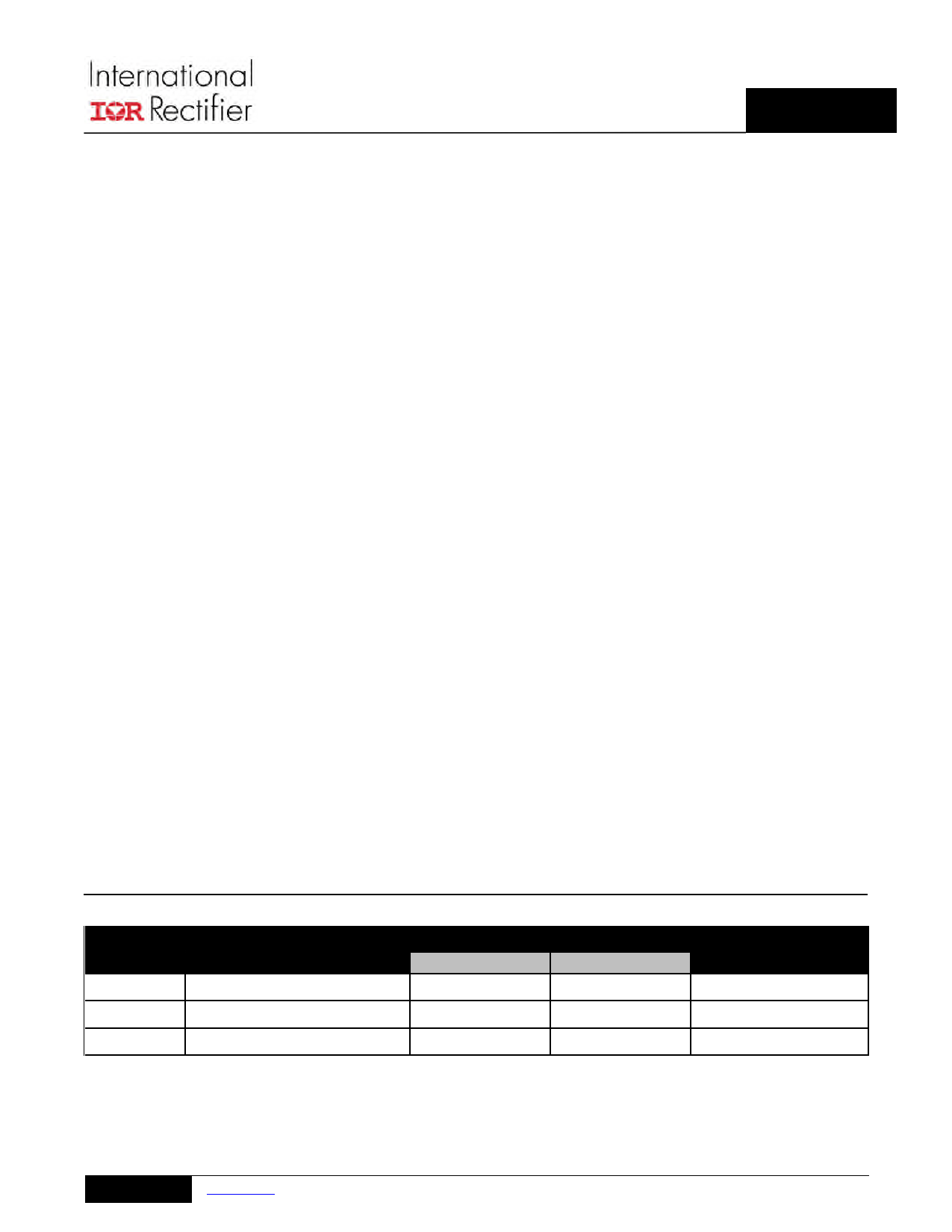
PARAMETER
Loop1 Iin Resolution Reporting-I2C1
Loop2 Iin Resolution Reporting-I2C1
P_in Resolution Reporting-PMBUS1
P_out Resolution Reporting-PMBUS1
Temperature Range Reporting1
Temperature Accuracy Reporting1
Temperature Range Reporting1
Temperature Accuracy Reporting1
Temperature Resolution Reporting1
Fault Protection
OVP Threshold During Start-up
(until output reaches 1V)
OVP Operating Threshold1
(programmable)
OVP Filter Delay1
Output UVP Threshold1 (programmable)
Fast OCP Range (per phase)1
Fast OCP Filter Bandwidth1
Slow OCP Filter Bandwidth1
SYMBOL
OCP System Accuracy1
PIN_ALERT# Bandwidth
VR_HOT Range1
OTP Range1, 2
Dynamic Phase Control
Current Filter Bandwidth1
Timing Information
Automatic Configuration from MTP1
Automatic Trim Time1
EN Delay (to ramp start) 1
VID Delay (to ramp start) 1
VRDY Delay1
Notes:
1 Guaranteed by design.
2 OTP max setting with NTC TEMP SENSE is 134°C.
t3-t2
t4-t3
CONDITIONS
IR3555 mode
IR3555 mode
At 100°C, with ideal NTC
MIN TYP MAX UNIT
- 0.125 - A
- 0.0625
-
A
- 0.5
-W
- 0.5
-W
0 - 158 °C
3.5 -
3.5 %
0 - 134 °C
-4 -
4%
-1
- °C
Selectable
-
1.2, 1.275,
1.35, 2.5
Relative to VID
- 50 to 400
- 160
Relative to VID
- 50 to 400
- 0 to 62
- 60
Selectable
0.69, 1.39,
-
2.78, 5.55,
11.1, 22.2,
44.6, 89.5
System excluding DCR/sense
resistor
-
±2
2000
- 64 to 127
OTP Range (added to
VR_HOT level)
- 0 to 31
-
-
-
-
-
-
-
-
-
-
V
mV
ns
mV
A
kHz
Hz
%
Hz
°C
°C
For Phase drop
-4
- kHz
3.3V ready to end of
configuration
Loop bandwidth dependent
After reaching Boot voltage
-
-
-
-
-
0.4
2
3
5
20
ms
ms
- µs
- µs
- µs
11 www.irf.com | © 2016 International Rectifier
February 8, 2016 | V1.5
11 Page | ||
| Páginas | Total 30 Páginas | |
| PDF Descargar | [ Datasheet IR35203.PDF ] | |
Hoja de datos destacado
| Número de pieza | Descripción | Fabricantes |
| IR35201 | 8+0/7+1/6+2 Dual Output Digital Multi-Phase Controller | International Rectifier |
| IR35203 | 6+1 Dual Output Digital Multi-Phase Controller | International Rectifier |
| IR35204 | 3+1 Dual Output Digital Multi-Phase Controller | International Rectifier |
| Número de pieza | Descripción | Fabricantes |
| SLA6805M | High Voltage 3 phase Motor Driver IC. |
Sanken |
| SDC1742 | 12- and 14-Bit Hybrid Synchro / Resolver-to-Digital Converters. |
Analog Devices |
|
DataSheet.es es una pagina web que funciona como un repositorio de manuales o hoja de datos de muchos de los productos más populares, |
| DataSheet.es | 2020 | Privacy Policy | Contacto | Buscar |
