|
|
|
PDF AD9144 Data sheet ( Hoja de datos )
| Número de pieza | AD9144 | |
| Descripción | Digital-to-Analog Converter | |
| Fabricantes | Analog Devices | |
| Logotipo | ||
Hay una vista previa y un enlace de descarga de AD9144 (archivo pdf) en la parte inferior de esta página. Total 30 Páginas | ||
|
No Preview Available !
Data Sheet
Quad, 16-Bit, 2.8 GSPS, TxDAC+®
Digital-to-Analog Converter
AD9144
FEATURES
Supports input data rate >1 GSPS
Proprietary low spurious and distortion design
6-carrier GSM IMD = 77 dBc at 75 MHz IF
SFDR = 82 dBc at dc IF, −9 dBFS
Flexible 8-lane JESD204B interface
Support quad or dual DAC mode at 2.8 GSPS
Multiple chip synchronization
Fixed latency
Data generator latency compensation
Selectable 1×, 2×, 4×, 8× interpolation filter
Low power architecture
Input signal power detection
Emergency stop for downstream analog circuitry protection
Transmit enable function allows extra power saving
High performance, low noise phase-locked loop (PLL) clock
multiplier
Digital inverse sinc filter
Low power: 1.6 W at 1.6 GSPS, 1.7 W at 2.0 GSPS,
full operating conditions
88-lead LFCSP with exposed pad
APPLICATIONS
Wireless communications
3G/4G W-CDMA base stations
Wideband repeaters
Software defined radios
Wideband communications
Point-to-point
Local multipoint distribution service (LMDS) and
multichannel multipoint distribution service (MMDS)
Transmit diversity, multiple input/multiple output (MIMO)
Instrumentation
Automated test equipment
GENERAL DESCRIPTION
The AD9144 is a quad, 16-bit, high dynamic range digital-to-
analog converter (DAC) that provides a maximum sample rate
of 2.8 GSPS, permitting a multicarrier generation up to the
Nyquist frequency. The DAC outputs are optimized to interface
seamlessly with the ADRF6720 analog quadrature modulator
(AQM) from Analog Devices, Inc. An optional 3-wire or 4-wire
serial port interface (SPI) provides for programming/readback
of many internal parameters. Full-scale output current can be
programmed over a typical range of 13.9 mA to 27.0 mA. The
AD9144 is available in an 88-lead LFCSP.
TYPICAL APPLICATION CIRCUIT
QUAD MOD
ADRF6720
LPF
DAC
0°/90° PHASE
SHIFTER
DAC
JESD204B
SYNCOUTx±
SYSREF±
LO_IN MOD_SPI
QUAD MOD
ADRF6720
LPF
0°/90° PHASE
SHIFTER
AD9144
QUAD
DAC
DAC
DAC
JESD204B
SYNCOUTx±
LO_IN MOD_SPI
CLK±
Figure 1.
DAC
SPI
PRODUCT HIGHLIGHTS
1. Greater than 1 GHz, ultrawide complex signal bandwidth
enables emerging wideband and multiband wireless
applications.
2. Advanced low spurious and distortion design techniques
provide high quality synthesis of wideband signals from
baseband to high intermediate frequencies.
3. JESD204B Subclass 1 support simplifies multichip
synchronization in software and hardware design.
4. Fewer pins for data interface width with a serializer/
deserializer (SERDES) JESD204B eight-lane interface.
5. Programmable transmit enable function allows easy design
balance between power consumption and wake-up time.
6. Small package size with 12 mm × 12 mm footprint.
Rev. A
Document Feedback
Information furnished by Analog Devices is believed to be accurate and reliable. However, no
responsibility is assumed by Analog Devices for its use, nor for any infringements of patents or other
rights of third parties that may result from its use. Specifications subject to change without notice. No
license is granted by implication or otherwise under any patent or patent rights of Analog Devices.
Trademarksandregisteredtrademarksarethepropertyoftheirrespectiveowners.
One Technology Way, P.O. Box 9106, Norwood, MA 02062-9106, U.S.A.
Tel: 781.329.4700
©2014 Analog Devices, Inc. All rights reserved.
Technical Support
www.analog.com
1 page 
AD9144
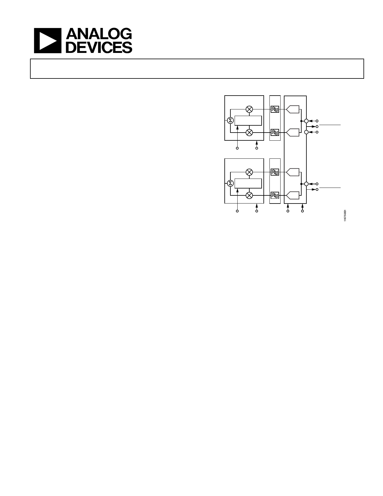
FUNCTIONAL BLOCK DIAGRAM
Data Sheet
VTT
SERDIN7±
SERDIN0±
PROTECT_OUT0
PROTECT_OUT1
SYNCOUT0+
SYNCOUT0–
SYNCOUT1+
SYNCOUT1–
SERDES
PLL
DACCLK
HB1
HB1
HB2
HB3
MODE CONTROL
HB2
HB3
COMPLEX
MODULATION
NCO
fDAC
÷4, ÷8
Q-GAIN
I-GAIN
Q-OFFSET
PHASE
ADJUST
I-OFFSET
FSC
DACCLK
FSC
OUT3+
OUT3–
OUT2+
OUT2–
HB1
HB2
HB3
MODE CONTROL
HB1
HB2
HB3
COMPLEX
MODULATION
NCO
fDAC
÷4, ÷8
Q-GAIN
I-GAIN
Q-OFFSET
PHASE
ADJUST
I-OFFSET
FSC
DACCLK
FSC
SYNCHRONIZATION
LOGIC
CONFIG
REGISTERS
CLOCK DISTRIBUTION
AND
CONTROL LOGIC
SERIAL
I/O PORT
POWER-ON
RESET
PLL_CTRL
DACCLK
PLL_LOCK
DAC
ALIGN
DETECT
DAC PLL
REF
AND
BIAS
SYSREF
Rx
CLK
Rx
OUT1+
OUT1–
OUT0+
OUT0–
I120
SYSREF+
SYSREF–
CLK+
CLK–
Figure 2.
Rev. A | Page 4 of 125
5 Page 
AD9144
Data Sheet
AC SPECIFICATIONS
AVDD33 = 3.3 V, SIOVDD33 = 3.3 V, IOVDD = 1.8 V, DVDD12 = 1.2 V, CVDD12 = 1.2 V, PVDD12 = 1.2 V, SVDD12 = 1.2 V,1 VTT = 1.2 V,
TA = 25°C, IOUTFS = 20 mA, unless otherwise noted.
Table 9.
Parameter
SPURIOUS-FREE DYNAMIC RANGE (SFDR)
fDAC = 983.04 MSPS
fDAC = 983.04 MSPS
fDAC = 1966.08 MSPS
fDAC = 1966.08 MSPS
TWO-TONE INTERMODULATION DISTORTION (IMD)
fDAC =983.04 MSPS
fDAC = 983.04 MSPS
fDAC = 1966.08 MSPS
fDAC = 1966.08 MSPS
NOISE SPECTRAL DENSITY (NSD), SINGLE-TONE
fDAC = 983.04 MSPS
fDAC = 1966.08 MSPS
W-CDMA FIRST ADJACENT CHANNEL LEAKAGE
RATIO (ACLR), SINGLE CARRIER
fDAC = 983.04 MSPS
fDAC = 983.04 MSPS
fDAC = 1966.08 MSPS
W-CDMA SECOND ACLR, SINGLE CARRIER
fDAC = 983.04 MSPS
fDAC = 983.04 MSPS
fDAC = 1966.08 MSPS
Test Conditions/Comments
−9 dBFS single-tone
fOUT = 20 MHz
fOUT = 150 MHz
fOUT = 20 MHz
fOUT = 170 MHz
−9 dBFS
fOUT = 20 MHz
fOUT = 150 MHz
fOUT = 20 MHz
fOUT = 170 MHz
0 dBFS
fOUT = 150 MHz
fOUT = 150 MHz
0 dBFS
fOUT = 30 MHz
fOUT = 150 MHz
fOUT = 150 MHz
0 dBFS
fOUT = 30 MHz
fOUT = 150 MHz
fOUT = 150 MHz
Min Typ Max Unit
82 dBc
76 dBc
81 dBc
69 dBc
90 dBc
82 dBc
90 dBc
81 dBc
−162
−163
dBm/Hz
dBm/Hz
82 dBc
80 dBc
80 dBc
84 dBc
85 dBc
85 dBc
1 SVDD12 = 1.3 V for all fDAC = 1966.08 MSPS conditions in Table 9.
Rev. A | Page 10 of 125
11 Page | ||
| Páginas | Total 30 Páginas | |
| PDF Descargar | [ Datasheet AD9144.PDF ] | |
Hoja de datos destacado
| Número de pieza | Descripción | Fabricantes |
| AD9142 | Digital-to-Analog Converter | Analog Devices |
| AD9142A | Digital-to-Analog Converter | Analog Devices |
| AD9144 | Digital-to-Analog Converter | Analog Devices |
| AD9146 | TxDAC Digital-to-Analog Converter | Analog Devices |
| Número de pieza | Descripción | Fabricantes |
| SLA6805M | High Voltage 3 phase Motor Driver IC. |
Sanken |
| SDC1742 | 12- and 14-Bit Hybrid Synchro / Resolver-to-Digital Converters. |
Analog Devices |
|
DataSheet.es es una pagina web que funciona como un repositorio de manuales o hoja de datos de muchos de los productos más populares, |
| DataSheet.es | 2020 | Privacy Policy | Contacto | Buscar |