|
|
PDF AD9006 Data sheet ( Hoja de datos )
| Número de pieza | AD9006 | |
| Descripción | A/D Converter | |
| Fabricantes | Analog Devices | |
| Logotipo |  |
|
Hay una vista previa y un enlace de descarga de AD9006 (archivo pdf) en la parte inferior de esta página. Total 15 Páginas | ||
|
No Preview Available !
ANALOG DEVICES FAX-ON-DEMANDHOTLINE - Page 16
,. ANALOG
W DEVICES
HighSpeed6-Bit
AIDConverters
I AD9006/AD9016I
FEATURES
FUNCTIONAL BLOCK DIAGRAM
500MSPS Encode Rate
Very Low Input Capacitance: 8pF
3OdBSNR @ 200M Hz Analog Input
MIL-STD-883 Available
Bipolar Input Range (:t1V)
Demultiplexed Outputs (AD9016)
Mll-STD-883-Compliant Versions Available
DD ., Dol 'NVERT
.
MS. !NVERT "
~A~~~Z~1
to
..09016
OUTI'tJT
LATCHES
'8) OVERFLOW A
BAN' A
APPLICATIONS
Radar Warning Receivers
Electronic Countermeasures
Transient Recorders
"Smart" Munitions
Digital Oscilloscopes
OBSGENERAL DESCRIPTION
The AD9006 and AD9016 are 6-bit, ultrahigh speed analog-ro-
Odigital converters. Both are fabricated in an advanced bipolar
process, assuring exceptionally wide analog input bandwidth,
Land encode rates up to SOOMSPS.Functionally, the AD9006
Eand AD9016 use "flash" architecture; the outputs of 64 parallel
comparator stages are decoded to drive a bank of ECL output
TElatches.
""
:,,,, I
I
I
I
I
L
~----
(Dotted Area Not Included in AD9006)
The AD9006 and AD9016 are available as commercial tempera-
ture range devices: 0 to + 70°C; and military temperatUre range
The AD9006 features a bipolar analog input range (:t IV). Out-
devices: - 55°C to + 125°c. Both versions are offered in a ce-
put data is provided in a single 6-bit data bank; the data is ECL
compatible and also includes complementary Data Ready signals
and an overflow bit. ECL-Ievel control pins allow the user to
ramic 68-pin LCC, and a ceramic 68-pin leaded package.
The AD9006/AD9016 are available in versions compliant with
invert the MSB and/or LSBs. The AD9006 exhibits excellent
SNR performance (30dB SNR Ca.2:00MHz input), and requires
less than two watts of power.
MIL-STD-883. Refer to the Analog Devices Military Products
Databook or current AD9006/AD9016/883B data sheet for de-
tailed specifications
In the AD9016, the performance and features of the AD9006
are combined with on-board demultiplexing circuits. Output
data of the AD9016 are demultiplexed to two 6-bit data banks,
each of which includes a Data Ready signal and overflow bit.
REV.A
Information furnished by Analog Devices is believed to be accurate and
reliable. However. no responsibility is assumed by Analog Devices for its
use, nor for any infringements of patents or other rights of third parties
which may result from its use. No license is granted by implication or
otherwise under any patent or patent rights of Analog Devices.
One Technology Way, P.O. Box 9106. Norwood. MA 02062.9106. U.S.A.
Tel: 617/329-4700
Fax: 617/326-8703
Twx: 710/394-6577
Telex: 924491
Cable: ANALOG NORWOODMASS
1 page 
-ANALOG DEVICES fAX-ON-DEMAND HOTLINE
Page 20
.. i':':' i!:
- -I d 8 ""Z~.~""g»'z,z++iu:i«8z~z~1.~2.z~o»:;/5uoz"u"g~"
'" i!I
z.\ ..z...
AD9006/AD9016
;. :+:3i:
.. g~d"!~<!~>~-giL0!8.!."~<>g~~~t3~~~~I"! ,~<0!~:
DiGITAL -v.
DiGITAL -v,
OVERFLOWINHftIIT
BIT INVERTIMSB'
0,-0. INVERT
GROUND
GROUND
NC
O\l£RFLOW
He
D,IMSB'
He
0,
He
AO9006
TOP VIEW
INol to Sca'.1
MIDSCALEv.,.,
HYSTERESIS
NC
GROUND
GROUND
He
He
NC
NC
NC
NC
NC
NC
He
DiGITAL -v.
OtGITAL -v.
OVERfLOW INHIBjT
BIT "'V~RT IMSB'
D..,<>,IN\IERT
GROUND
GROUND
NC
OVERFLOW.
He
D~ IM58'
NC
Doo
NC
AD9016
TOP VIEW
INo. to Sc.'"
MIDSCALE VM,
HYSTERESIS
He
GROUND
GROUND
He
DATAREAOT,
He
DooILSB'
Ne
D,.
Ne
D..
NC
D, NC
He NC
0, He
O~i'"~~:~5;;":>~:)~;;I~I
~~i~
< :I;
"4 ~ ;1:;12288 ~ ~
O J IU ~.~. !"i"~!!ia...",
.. "
I
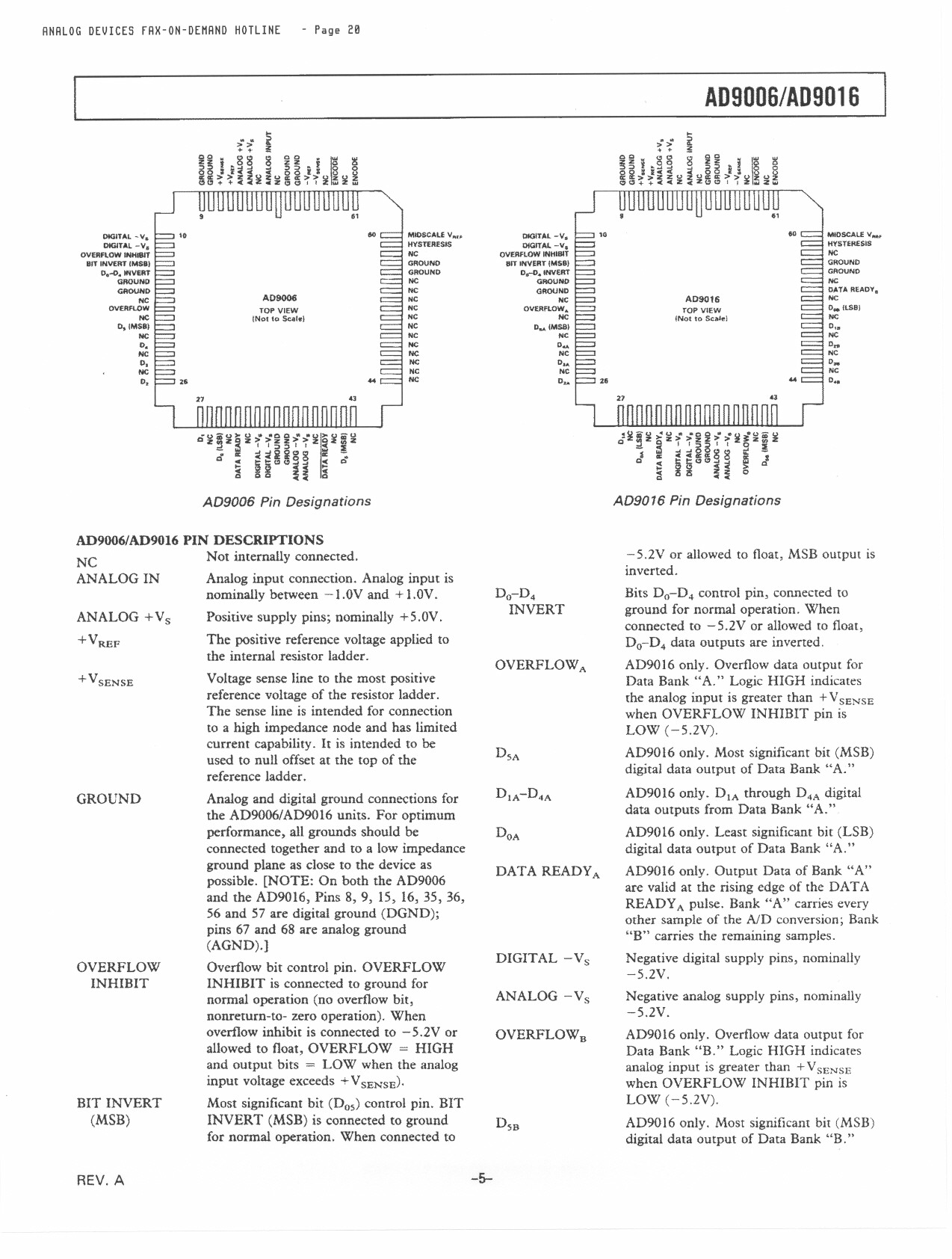
BAD9006 Pin Designations
SAD9006/AD9016 PIN DESCRIPTIONS
ONC
LANALOG IN
Not internally connected.
Analog input connection. Analog input is
nominally between -1. 0V and + 1.OV.
EANALOG +Vs
Positive supply pins; nominally +5.0V.
TE+VREF
The positive reference voltage applied to
the internal resisror ladder.
D,.
NC
D,.
Do-D4
INVERT
~.,,- u 'u. "'0
-Z Z>Z»Zi!;
>" >"z">":z<",.z>ti;,,
" "I I io I I 0 :Ii
!" 11°t3.H. '" J
AD9016 Pin Designations
0..
NC
D..
-5.2V or allowed to float, MSB outpUt is
inverted.
Bits Do-D4 control pin, connected to
ground for normal operation. When
connected to -5.2V or allowed to float,
Do-D4 data oUtputs are inverted.
OVERFLOW A
AD9016 only. Overflow data output for
+VSENSE
Voltage sense line to the most positive
Data Bank" A." Logic HIGH indicates
reference voltage of the resistor ladder.
The sense line is intended for connection
the analog input is greater than + VSENSE
when OVERFLOW INHIBIT pin is
to a high impedance node and has limited
LOW (-5.2V).
current capability. It is intended to be
used to null offset at the rop of the
reference ladder.
DSA
AD9016 only. Most significant bit (MSB)
digital data oUtput of Data Bank "A."
GROUND
Analog and digital ground connections for
the AD9006/AD9016 units. For optimum
D'A-D4A
AD9016 only. D'A through D4Adigital
data oUtputs from Data Bank "A."
performance, all grounds should be
DOA
AD9016 only. Least significant bit (LSB)
connected together and to a low impedance
digital data outpUt of Data Bank "A."
OVERFLOW
INHIBIT
ground plane as close to the device as
possible. [NOTE: On both the AD9006
and the AD9016, Pins 8, 9, IS, 16, 35, 36,
56 and 57 are digital ground (DGND);
pins 67 and 68 are analog ground
(AGND).]
Overflow bit control pin. OVERFLOW
INHIBIT is connected to ground for
normal operation (no overflow bit,
nonretUrn-to- zero operation). When
overflow inhibit is connected to -5.2V or
allowed to float, OVERFLOW = HIGH
and output bits = LOW when the analog
input voltage exceeds + VSENSE)'
DATA READYA
DIGITAL -Vs
ANALOG -Vs
OVERFLOW B
AD9016 only. Output Data of Bank "An
are valid at the rising edge of the DATA
READY A pulse. Bank "An carries every
other sample of the ND conversion; Bank
"B" carries the remaining samples.
Negative digital supply pins, nominally
-5.2V.
Negative analog supply pins, nominally
-5.2V.
AD9016 only. Overflow data output for
Data Bank "R." Logic HIGH indicates
analog inpUt is greater than + VSENSE
when OVERFLOW INHIBIT pin is
BIT INVERT
Most significant bit (Dos) control pin. BIT
LOW (-5.2V).
(MSB)
INVERT (MSB) is connected to ground
for normal operation. When connected to
D5B
AD9016 only. Most significant bit (MSB)
digital data output of Data Bank "B."
REV. A
-5-
5 Page 
-ANALOGDEVICES fAX-ON-DEMAND HOTLINE
Page ~6
AD9006/AD9016
0
II
-2 FUNDAMENTAL
.-
-4
-6
A1N=%O.75V (750/. of :t1V FS)
-8
.....
'-.......
"-
-10' 1 !
FUNDAMENTAL
..--
-12
/"
",
-14
'-
"-.....---
-18
A,N= :to.25V125%of :t IV FSI
-\8 I
~ -10
-12
-14
-16
-
/ 'x'
-IOFFSET \I
I --....
-20
-22 : ./
-24
,i
./ 'r '"
,/' \
3RD HARMONIC
-26
.../
J
2ND HARMONIC
--! 0. Y /-1S
II
3RDHARMONIC
t
tI : / iI I
-20
50 100 1SO 200 250 300 350 400 450 500 550
-INPUT FREQUENCY MHz
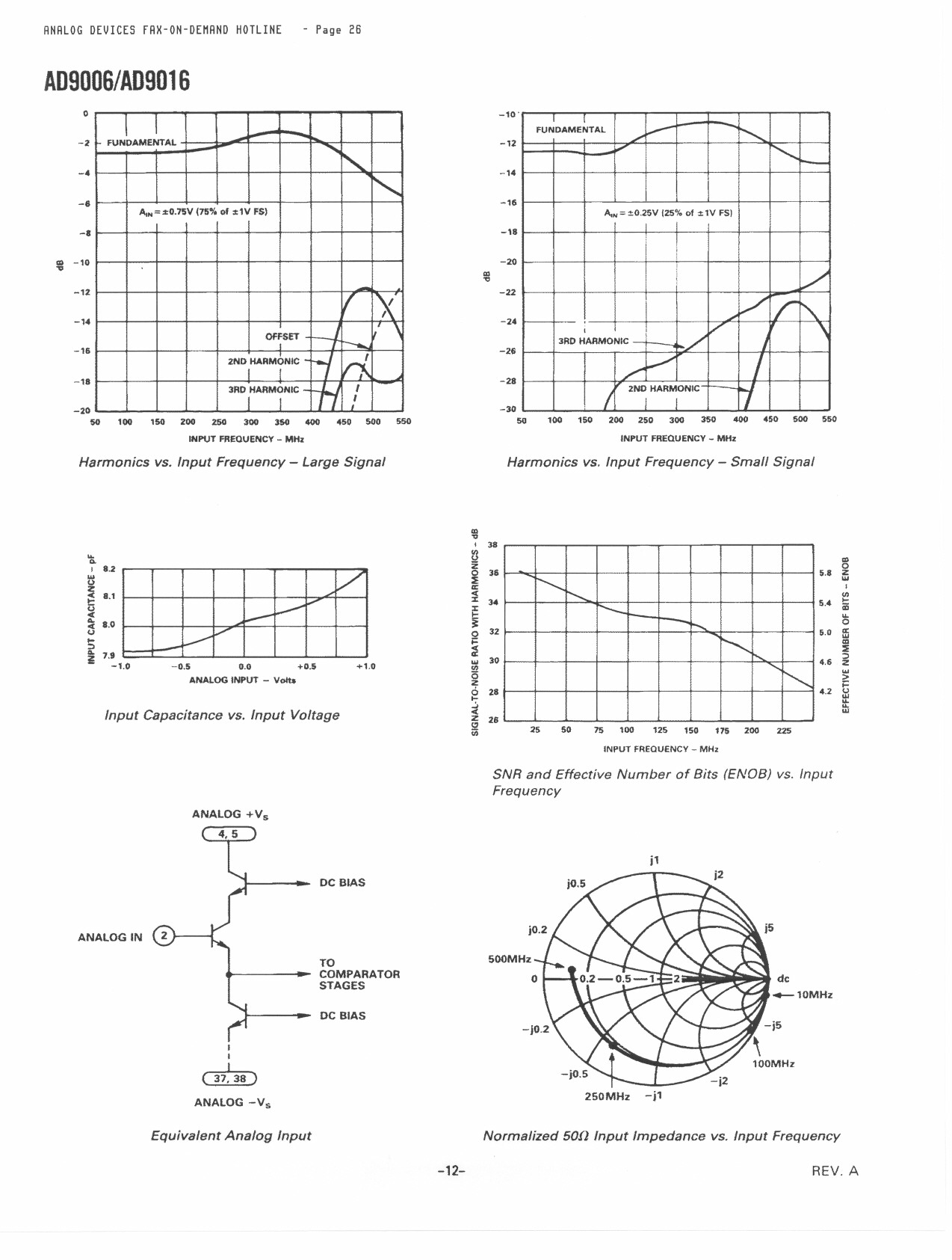
-Harmonics vs. Input Frequency Large Signal
O~~ BSO8.2
L r--4I::i:: 8.1
E-:ut 8.0
T;;
E~ 7'~1.0
-0.5 0.0 +0.5
ANALOG INPUT - V-
+1.0
-28
-30
50
2ND HARMONIC
jI
100 1SO 200 250 300 350 400 450 500 550
INPUT FREQUENCY .. MHz
Harmonics vs. Input Frequency - Small Signal
~
. 38
!3
Z
~r«r 36
%:..r. 34
~
0 32
;::
~
.'".. 3D
z(5
"""""""
............
...-
.........
........
'"
0
5.8 'Z.".,.
5.4 ~
...
0
5,0 fcDfi
::E
~4.6
.>..
;::
Input Capacitance vs. Input Voltage
g 28
.<j
~ 28
0;
25 50 75 100 125 150 175 200 225
4,2 :rl
:..t.:
INPUT FREQUENCY.. MHz
SNR and Effective Number of Bits (ENGB) vs. Input
Frequency
DC BIAS
jl
ANALOG IN
TO
COMPARATOR
STAGES
DC BIAS
I
I
I
( 37. 38 )
ANALOG -Vs
Equivalent Analog Input
500MHz
0
de
_10MHz
250MHz -j1
100MHz
Normalized 50fllnput Impedance vs. Input Frequency
-12- REV. A
11 Page | ||
| Páginas | Total 15 Páginas | |
| PDF Descargar | [ Datasheet AD9006.PDF ] | |
Hoja de datos destacado
| Número de pieza | Descripción | Fabricantes |
| AD9000 | High Speed 6-Bit A/D Converter | Analog Devices |
| AD9002 | High Speed 8-Bit Monolithic A/D Converter | Analog Devices |
| AD9006 | A/D Converter | Analog Devices |
| AD9007 | A/D Converter | Analog Devices |
| Número de pieza | Descripción | Fabricantes |
| SLA6805M | High Voltage 3 phase Motor Driver IC. |
Sanken |
| SDC1742 | 12- and 14-Bit Hybrid Synchro / Resolver-to-Digital Converters. |
Analog Devices |
|
DataSheet.es es una pagina web que funciona como un repositorio de manuales o hoja de datos de muchos de los productos más populares, |
| DataSheet.es | 2020 | Privacy Policy | Contacto | Buscar |
